AddThis

Bookmark and Share
Showing posts with label engineering projects abstract. Show all posts

Friday, 2 December 2011

Smart Fan: A Human Tracking Fan System

The two PIR sensors are separated in the middle. The purpose of this is to separate the sensors’ field of view.

When a sensor detects the right amount of infra-red light a comparator output goes high. We use the microcontroller to generate an interrupt on the comparator’s rising edge. The interrupt then signals a task that begins rotating the platform’s motor. The rotation is clockwise if the left sensor has detected a person or counter clockwise if the right sensor has detected a person. Once the fan is directed at the person’s location, there is just enough infra-red light in the second sensor’s field of view to trigger its comparator. This generates an interrupt that signals a task to either stop or redirect the motor, depending on the setting. At this point the customer is nice and cool without exerting any effort.

An example of the fan’s operation is illustrated in the block diagram below.


Saturday, 19 November 2011

grid tied inverter,grid interactive inverter

grid-tie inverter (GTI) is a special type of inverter that converts direct current(DC) electricity into alternating current(AC) electricity and feeds it into an existing electrical grid. GTIs are often used to convert direct current produced by many renewable energy sources, such as solar panels or small wind turbines, into the alternating current used to power homes and businesses. The technical name for a grid-tie inverter is "grid-interactive inverter". They may also be called synchronous inverters. Grid-interactive inverters typically cannot be used in standalone applications where utility power is not available.

A recent development in renewable energy technology is 'grid-interactive' or two way grid interconnection. These systems use sophisticated control equipment so that when your renewable energy system produces more power than you need, the excess power is fed back into the grid i.e. power is exported to the grid. When your system doesn't produce or have enough power, then you draw power from the grid. Some electricity retailers offer 'net billing' arrangements, so that they buy the electricity you produce at the same price as they sell their electricity to you. The renewable electricity is produced as Direct Current (DC). The DC electricity from the panels passes through a grid-interactive inverter, which converts the DC electricity into Alternating Current (AC), which is the type of electricity supplied by the grid

This AC electricity is then used by any appliances operating in the house. If more electricity is produced than the house needs then the excess will be fed into the main electricity grid. Conversely, when the renewable system is not generating enough electricity to power the house, the house will draw power from the grid. Grid interactive systems eliminate the need for a battery backup for when the sun doesn't shine (if it’s a solar system) or the wind doesn't blow (if it’s a wind turbine). In effect, the grid serves as your battery. This means that maintenance costs for your system will be less. It should be noted that without battery storage, a grid connected system will shut down when there is no power on the grid.


Features
  • Grid interactive systems
  • Low Maintenance Costs
  • Eco-Friendly

Tuesday, 20 July 2010

Blood Pressure Monitor Block Diagram and Design Considerations

Design Considerations:

Blood pressure monitors can use Korotkoff, Oscillometry, or Pulse Transit Time methods to measure blood pressure. They employ a pressure cuff, pump, and transducer to measure the blood pressure and heart rate in three phases: Inflation, Measurement, and Deflation. They include an LCD, memory recall, selection buttons, power management, and USB interface.

The pressure transducer produces the output voltage proportional to the applied differential input pressure. The output voltages of the pressure transducer range from 0 to 40 mV, which needs to be amplified so that the output voltage of the DC amplifier has a range from 0 to 5V. This is why, we need a high-gain amplifier. Then the signal from the DC amplifier will be passed on to the band-pass filter. The DC amplifier amplifies both DC and AC component of the signal. The filter is designed to have large gain at around 1-4 Hz and attenuate any signal that is out of the pass band. The AC component from filter is important for determining when to capture the systolic/diastolic pressures and heart rate of the patient. The final stage of the front end is an AC coupling stage, after which the signal is sent to analog to digital converters, and digitized.

The digital measurements of pressure and heart rate are performed by the microprocessor. Measurements results are stored in EEPROM or FLASH memory as a data log that can be uploaded to a PC via USB. The analog circuit is used to amplify both the DC and AC components of the output signal of pressure transducer so that we can use the MCU to process the signal and obtain useful information about the patient’s health.

Block Diagram:


Download Useful Technical Documents:

EEPROM Emulation With the TMS320F28xxx DSCs

A Single-Chip Pulsoximeter Design Using the MSP430

Source: Texas Instruments

Digital Signal Processing Biometrics Applications

Introduction To Digital Signal Processing

DSP or Digital Signal Processing is the technology of manipulating analog information that has been obtained from sources such as sound or photography data that have been converted into digital format. It uses complex mathematical formulas to the raw data to form another type of modified output. It uses the compression technique to transmits and display information effectively.

Products such as video conferencing uses complex hardware and software DSP processing. Many of these products have dedicated DSP chips where they are placed into the sound card that provide extra audio processing power to reduce the loading of processing in the CPU. In the total system solution, the DSP technology collects the raw data, process it, compress it, trasmit it and display it once again in the various digital display devices.

Digital Signal Processing In Biometrics

Biometrics is the technology used to analyze biological data. Its most recent application is in the area of security where the biological data of a person is used for personal identification and authentication before the person is allowed to proceed to enter a building or do any business transactions. Fingerprint, iris scan and facial features are among some of the human biometrics used.

The development of single chip DSP microcontroller that processes the electrical signals generated by the transducers such as digital camera CCD devices and fingerprint sensors have helped to speed up the processing power and hence make authentication easy and efficient.

One of the industry leader in DSP technology is Texas Instruments which have developed dedicated microcontroller for DSP application. The technology that have been developed in Biometrics are discussed in great details and is a great source of design references for students or even electronics designers who are keen to develop a biometrics based DSP system. The document can be obtained from Digital Signal Processing Texas Instrument Website.

Monday, 19 July 2010

HVAC Thermostat

Introduction To HVAC Thermostat

HVAC thermostat has been one of the common device used in residential and industrial buildings to control the temperature of a space be it a warehouse, a room, a hall or an office. This thermostat project will focus on the heating control of a space that uses electric heater as its source of heating. It basically consists of a comparator that controls the ON and OFF of the electric heater based on the sensor temperature.

The control of the fan speed is usually hardwired with two speed or three speed motors and is incorporated into the thermostat. The temperature range of this thermostat is from 5 Celcius to 30 Celcius with a tolerance of approximately 3 degree Celcius. Hence, only non critical tolerance control of temperature control such as a room can be used.

Circuit Description

The circuit diagram shows the configuration of the HVAC thermostat. The LM358 Op Amp is used as a comparator to sense the inputs of the reference voltage (PIN 3) and room temperature (PIN 2). The thermistor used is a NTC (negative temperature coefficient) type where its resistance will drop when the temperature increases and vice versa. It has a resistance of 20K ohm at 25 degree Celcius. When the room temperature drops, the thermistor resistance will go up and hence the output of the operational amplifier will be low. This cause the relay to turn OFF and the heater will conduct until the temperature of the room rises again.


The circuit is calibrated using variable resistor VR1. Set the lever of the slide potentiometer or rotary potentiometer VR2 to 25 Celcius location. Place the thermistor at a space where the temperature is at 25 Celcius. By varying VR1, set the resistance at the position between the ON and OFF of the relay. Use a suitable contact relay rating according to the load of the heater.

Parts List


Analog Timing Light Project

Timing Light Project

This analog timing light project uses RC circuit as a delay OFF timer to control the duration an incandescent light turns ON. When the accuracy of a timer is not critical, the use of RC circuit is a good choice as it is more cost effective and simple. Once the normally open switch SW is pressed, the light will turn ON for a duration of 10 - 20 seconds before it turns OFF. The duration of the turn ON time can be varied by varying the values of R1, R2 and E1.

Schematic Diagram

The schematic of the project is as shown below.


When SW is pressed, the base of the transistor Q1 is forward bias and it turns ON. This turns ON the 12V relay that is connected to the transistor. The contact of the relay RLY must be able to withstand the current of the load. At the same time, the electrolytic capacitor E1 is being charged to a voltage of approximately 0.7V.

Once SW is released, E1 will discharged through resistor R2 and the base of the transistor. After some time, When the voltage across E1 drops to approximately 0.5V, the transistor will turn OFF. This in turn will cause the relay to turn OFF and the incandescent light will turn OFF. The timing of the turn OFF can be changed by changing the values of E1, R1 and R2.

Parts List

The parts list of the project is as shown below.

Bar Graph LED Project

This bar graph LED battery level indicator project is based on LM3914 monolithic IC from National Semiconductor that senses the voltage levels of the battery and drives the 10 light emitting diodes based on the voltage level that is detected. It provides a linear analog display output and has a pin that can be configured to display the output in moving dot or bar graph. The current driving the LEDs is regulated and programmable hence limiting resistors are not required.


The schematic shows how the various components are connected. Switch S1 is used to change the display type from moving dot to bar graph type. When S1 is ON, the display type is bargraph but when it is OFF the display changes to moving dot type. VR1 is used to set the lower limit of the display. By using a variable DC power supply, set the VBAT to 10.5V. Adjust VR1 until the LED L1 turns ON. Next, set the VBAT to 15V, adjust VR2 until all the LEDs turn ON (When S1 is ON). The specifications of LM3914 can be obtained from National Semiconductor Website.


Parts List

Smart Cameras in Embedded Systems

Introduction
A smart camera performs real-time analysis to recognize scenic elements. Smart cameras are useful in a variety of scenarios: surveillance, medicine, etc.We have built a real-time system for recognizing gestures. Our smart camera uses novel algorithms to recognize gestures based on low-level analysis of body parts as well as hidden Markov models for the moves that comprise the gestures. These algorithms run on a Trimedia processor. Our system can recognize gestures at the rate of 20 frames/second. The camera can also fuse the results of multiple cameras

Overview

Recent technological advances are enabling a new generation of smart cameras that represent a quantum leap in sophistication. While today's digital cameras capture images, smart cameras capture high-level descriptions of the scene and analyze what they see. These devices could support a wide variety of applications including human and animal detection, surveillance, motion analysis, and facial identification.

Video processing has an insatiable demand for real-time performance. Fortunately, Moore's law provides an increasing pool of available computing power to apply to real-time analysis. Smart cameras leverage very large-scale integration (VLSI) to provide such analysis in a low-cost, low-power system with substantial memory. Moving well beyond pixel processing and compression, these systems run a wide range of algorithms to extract meaning from streaming video.

Because they push the design space in so many dimensions, smart cameras are a leading-edge application for embedded system research.

Detection and Recognition Algorithms

Although there are many approaches to real-time video analysis, we chose to focus initially on human gesture recognition-identifying whether a subject is walking, standing, waving his arms, and so on. Because much work remains to be done on this problem, we sought to design an embedded system that can incorporate future algorithms as well as use those we created exclusively for this application. Our algorithms use both low-level and high-level processing. The low-level component identifies different body parts and categorizes their movement in simple terms. The high-level component, which is application-dependent, uses this information to recognize each body part's action and the person's overall activity based on scenario parameters. Low-level processing The system captures images from the video input, which can be either uncompressed or compressed (MPEG and motion JPEG), and applies four different algorithms to detect and identify human body parts.

Region extraction: The first algorithm transforms the pixels of an image into an M ¥ N bitmap and eliminates the background. It then detects the body part's skin area using a YUV color model with chrominance values down sampled Nextthe algorithm hierarchically segments the frame into skin-tone and non-skin-tone regions by extracting foreground regions adjacent to detected skin areas and combining these segments in a meaningful way.

Contour following: The next step in the process involves linking the separate groups of pixels into contours that geometrically define the regions. This algorithm uses a 3 ¥ 3 filter to follow the edge of the component in any of eight different directions.

Ellipse fitting: To correct for deformations in image processing caused by clothing, objects in the frame, or some body parts blocking others, an algorithm fits ellipses to the pixel regions to provide simplified part attributes. The algorithm uses these parametric surface approximations to compute geometric descriptors for segments such as area, compactness (circularity), weak perspective invariants, and spatial relationships.

Graph matching: Each extracted region modeled with ellipses corresponds to a node in a graphical representation of the human body. A piecewise quadratic Bayesian classifier uses the ellipses parameters to compute feature vectors consisting of binary and unary attributes. It then matches these attributes to feature vectors of body parts or meaningful combinations of parts that are computed offline. To expedite the branching process, the algorithm begins with the face, which is generally easiest to detect.


Friday, 4 June 2010

Automatic car parking indicator using Microcontroller

Description:
Conventionally, car parking systems does not have any intelligent monitoring system. Parking lots are monitored by human beings. All vehicles enter into the parking and waste time for searching for parking slot. Sometimes it creates blockage. Condition become worse when there are multiple parking lanes and each lane have multiple parking slots.

Use of automated system for car parking monitoring will reduce the human efforts. Display unit is installed on entrance of parking lot which will show LEDs for all Parking slot and for all parking lanes. Empty slot will be indicated by glowing the respective LED.


Block Diagram:


Description:
We have used Infra Red transmitters and Receivers for each parking slot. The IR Receivers are connected to AVR microcontroller. IR rays are obstructed when a car is parked in any parking slot. Thus AVR will come to know that which slot is empty and which slot is full. We have chosen IR module instead of RF module because we want a receiver having line of sight communication with the transmitter. But RF does not require line of sight communication. And in case of LDR, there is scope for false triggering due to sunlight or headlight of car. So considering all these points we have finalized to use IR module. For transmitter section we are going to use IR LEDs driven by a 555 timer IC. Timer IC will generate a frequency of 38 KHz, which will be given to IR LED

Pick and Place robot

INTRODUCTION:
In this highly developing society; time and man power are critical constrains for completion of task in large scales. the automation is playing important role to save human efforts in most of the regular and frequently carried works e.g. most of the industrial jobs like welding, painting, assembly, container filling etc. one of the major and most commonly performed work is picking and placing of jobs from source to destination. For this purpose, ‘pick and place robot ‘maybe used.
The pick and place robot is a microcontroller based mechatronic system that detects the object, picks that object from source location and places at desired location. For detection of object, infrared sensors are used which detect presence of object as the transmitter to receiver path for infrared sensor is interrupted by placed object. As soon as robot senses presence of object, it moves towards object, picks it with end effectors, and moves along way gantry and finally place it on destination.
If another object causes interrupt, it again does the same job. Whole process is controlled by micro controller.

Block Diagram:

DESIGN SPECIFICATIONS:
ADC Interface ---- 4 channel (expandable) to detect object position.
Supply Voltage ---- 230V (AC).
8 bit microcontroller – P89V51RD2.
Motor interface – 3 motors : 2 motors in parallel.

MECHANICAL DESIGN:
This pick and place robot has two main mechanical components:
A] Robotic arm and end-effectors.
B] Gantry for moving the arm.

OPERATION OF ROBOT :
1. Initially we will assume the rest position of entire system, i.e. state when no object is placed.
2. At this stage, photo detector is having its output high, since receiver of sensor can receive photons from transmitter as no object I in its path to interrupt.
3. As soon as object is placed at the picking platform, the sensor gets interrupted and outputs low. This signal is sent to the microcontroller which is burnt with program which tells what operation is to be performed at this stage.
4. For understanding operation, let us rename the two motors used here. Let the name of gantry motor be M1 and that for end effecter motor is M2.
5. Now as microcontroller detects that object is placed, it moves motor M1 in say clockwise direction for a fixed time due to which whole arm moves towards picking platform.
6. As it reaches there, M1 stops and now motor M2 is started in say clockwise direction to hold the object by closing jaw. This motor also, is on for particular fixed time instant.
7. As M2 gets off, motor M1 is moved again in opposite (here anticlockwise) direction till the time it reaches the placing platform.
8. As it reaches placing platform, the motor M1 stops and M2 is switched ON in opposite (here anticlockwise) direction till it releases object properly on desired place.
9. If after this no object is detected, the robot is in rest position. Otherwise if another object is detected, steps from 3 are repeated till step 8.

BLOCK DIAGRAM DESCRIPTION:
I] ADC:
1. We are using an 8 bit ADC PCF 8591, which uses an I2C bus protocol. It has 4 analog input channels AIN1, AIN2, AIN3 & 1 analog output channel AOUT. > Pin no. 1 i.e. channel 1 is connected IR sensor.
2. Except for the micro controller AT 89V51RD2, there is no other peripheral device connected to the ADC. Hence the hardware address lines (A0, Al & A2) are grounded.
3. Pin no. 9 and 10 are serial data line (SDA) and serial clock line (SCL) respectively. Both lines must be connected to a positive supply through a pull-up resistor. These pins are connected to the P1.6 & P1.7 of the micro controller.
4. Here we are not feeding the OSC (pin no. 11) with an external clock Signal, but using the ON chip oscillator. Hence the EXT pin (pin no.12) is directly grounded.
5. Vref (pin no. 14) is connected to the 5 V regulated supply.
II] Microcontroller: 1. PORT 0: (PIN NO. 39- PIN NO. 32): P0.0— P0.7 of the micro controller is connected to the motor driver circuit.
2. Pin no. 9 is RESET pin, which is connected to the reset circuit.
3. Pin no. 9 and 10 of ADC are serial data line (SDA) and serial clock line (SCL) respectively. Both are connected to a positive supply through a pull-up resistor. These pins are connected to the P1.6 & P1.7 of the micro controller.
III] DRIVER CIRCUIT:
1. The L293 and L293D are quadruple high-current drivers.TheL293is designed to provide bidirectional drive currents of up to 1 A at voltages from 4.5 V to 36 V. The L293D is designed to provide bidirectional drive currents of up to 600-mA at voltages from 4.5 V to 36 V. Both devices are designed to drive inductive loads such as relays, solenoids, dc and bipolar stepping motors, as well as other high-current/high-voltage loads in positive-supply applications.
2. All inputs are TTL compatible. Each output is a complete totem-pole drive circuit, with a Darlington transistor sink and a pseudo-Darlington source. Drivers are enabled in pairs, with drivers 1 and 2 enabled by 1,2EN and drivers 3 and 4 enabled by 3,4EN.
3. When an enable input is high, the associated drivers are enabled and their outputs are active and in phase with their inputs. When the enable input is low, those drivers are disabled and their outputs are off and in the high-impedance state. With the proper data inputs, each pair of drivers forms a full-H (or bridge) reversible drive suitable for solenoid or motor applications.
4. A Vcc1 terminal, separate from Vcc2, is provided for the logic inputs to minimize device power dissipation.

APPLICATIONS:
1. It can be used in Production industry.
2. In mass production.
3. In Automobile Industry.
FUTURE SCOPE:
1. Bottle filling Plant.
2. Construction works.

REFERENCES:
1. Programming Microcontroller 8051 and customizing By Myke Predko
2. 8051 Microcontroller By Mazidi and Mazidi
3. 8051 Microcontroller By Kenneth Ayala

Component List
Sr no. Component Quantity Cost(Rs)
1 Transformer 12V, 1A 1 55
2 Diode 1N4007 4 5
3 Electrolytic capacitor 2200uf, 25V 1 3
4 Capacitor 100uf 2 5
5 IC 7805 1 8
6 IC 7812 1 8
7 Crystal 11.0592Mhz 1 20
8 IC L293d 1 95
9 P89V51RD2 1 125
10 PCF8591 1 125
11 IC Socket 40pin DIP 1 20
12 IC Socket 16pin DIP 2 10
13 2 pin connector 4 20
14 PCB 4*4 1 20
15 PCB 6*4 1 25
16 PCB 1 25
17 Resistors 5 3
18 Miscellaneous 10
19 Mechanical assembly 900

Landrover Robot Operated by Cellphone

Description:
In this project, the robot is controlled by a mobile phone that makes a call to the mobile phone attached to the robot.
In the course of a call, if any button is pressed, a tone corresponding to the button pressed is heard at the other end of the call.
This tone is called "Dual Tone Multiple-Frequency" (DTMF) tone. The robot perceives this DTMF tone with the help of the phone stacked on the robot.
The received tone is processed by the microcontroller with the help of DTMF decoder.
The microcontroller then transmits the signal to the motor driver ICs to operate the motors.
The metal detector circuit mounted on the robot detects any metal object around it.


Block Diagram:

Greenhouse Robot

Description in detail:
On the robot we have mounted a 12V battery as the power supply for the circuit and the motors.
When the user calls the mobile which is mounted on the robot the call is received by auto-answer mode.
As the call continues when the user presses a button on his handset the tone that is generated is decoded by the DTMF decoder and the command is passed to the microcontroller which is pre-programmed.
The Microcontroller then passes the command to the motor driver ICs for motion.
The metal detector when detects a metal and turns the buzzer on.

Applications: This robot can be used in the borders for disposing hidden land mines.
The robot can be used for reconnaissance or surveillance.
The robot can be used anywhere there is the service provider tower of the connection provided that is mounted on the robot.
The robot is small in size so can be used for spying.

Controller Area Network project

Description: Control Area Network controls the security of the Electronic equipments using the RS-485 protocol. We use CAN for Monitoring Sensors. Data can be stored in the System and the software is used for backup. We can get reports on hourly, weekly and monthly basis.
The Controller Area Network (CAN) bus is a multi-master message broadcast system that is suitable for systems where data contained in short messages are needed to be received at multiple locations simultaneously. Because messages are sent to all the nodes in a system, CAN is especially suited to systems where consistency in the received messages at all the receiving nodes is needed. In this case, all nodes are notified of the rejection, ensuring the data consistency across the network.
Messages are sent to all nodes, but their "message identifiers" indicate whether each node should act on the message. However, all nodes participate in indicating whether the message was sent correctly, increasing the reliability of the bus.
Designing and development process can be divided in to three Section.
1) Primarily Design
2) Embedded System
3) Monitoring Software

Block Diagram:

Controller Area Network

Description in detail: It mainly consist of following Modules
Module -1
This relates to Master circuits. (master Circuit)
Module -2
The module-2 is used to measure the RPM of the motor using the TACHOMETER which gives the voltages.
Module -3
The module-3 is used to measure of the Temperature of the motor using a TEMPERATURE SENSOR.
Module -4
The module-4 is used to rotate the angle of STEPPER MOTOR with the help of microcontroller programming

Remote Surveillance Vehicle using AVR ATmega16

Description:
In this project, the robot is controlled by a mobile phone that makes a call to the mobile phone attached to the robot.
In the course of a call, if any button is pressed, a tone corresponding to the button pressed is heard at the other end of the call.
This tone is called "dual tone multiple-frequency" (DTMF) tone. The robot perceives this DTMF tone with the help of the phone stacked on the robot.
The received tone is processed by the microcontroller with the help of DTMF decoder.
The microcontroller then transmits the signal to the motor driver IC"s to operate the motors.
The camera and micro-phone mounted on the robot will give the detailed information of where the robot is and who is around. The signal is then transmitted to the observer via audio/video transmitter-receiver.
The metal detector circuit mounted on the robot detects any metal object around it and transmits the signal wirelessly.


Block Diagram:

Friday, 21 May 2010

PROJECT ON WIRELESS DATA AND VOICE COMMUNICATION THROUGH INFRARED-LED

TITLE OF THE SYNOPSIS:-

“Conceptual designs development & demonstrations of a
WIRELESS DATA AND VOICE COMMUNICATION THROUGH INFRARED-LED”

OBJECTIVES:-

To Design a circuit of an electronic infrared communication system.
Develop new ideas to implement this circuit purposely.
To study the circuitry and different types of components & DTMF generator, DTMF decoder, op-amp and infrared-LED in the circuit.

INTRODUCTION

For years, infrared LED has been merely a system for piping light around corners and into the inaccessible places to allow the hidden to be lighted. But now, infrared LED has evolved into a system of significantly greater importance and use. Throughout the world, it is now being used to transmit voice, television and data signals as light waves. Its advantages as compared with conventional coaxial cable or twisted wire pairs are manifold. As a result, millions of dollars are being spent to put these light wave communication systems into operation.
One of the most interesting developments in recent years in the field of telecommunication is the use of laser light to carry information over large distances. It has been proved in the past decade that light wave transmission through laser light is superior than that achieved through wires and microwave links. Typically, infrared LED has a much lower transmission loss per unit length (0.15-5db/km) and is not susceptible to electromagnetic interference. Economically also, it serves our purpose. The ever increasing cost and the lack of space available in the congested metropolitan cities asks for advent of a less costly system.
The conventional telephonic systems use copper wires, which easily get oxidized and as such require high maintenance cost. The laser light being made of glass are non-reactive and hence economical. Also, the noise pick up by the copper wire or in electrical signals is quite substantial whereas in laser light, the noise pick up is negligible.

Basic elements of a infrared LED system

Applications
(i) Applications for video transmission include high quality video Trunked from studio Transfeter, Broadcast CATV video, Video Trunking within city or between cities, Baasedand Video for closed.

BLOCKDIAGRAM

block diagram not visible due to image format problems hope to remove this problem soon………..

CONSTRUCTION AND WORKING

MIKE: Its converts sound signals into electrical signals.

AMPLIFIER (A): Signals from mike are amplified so that it can drive to infrared-LED.

INFRARED-LED: It carries signals.

PHOTO TRANSISTOR: The electrical signals are regained from the optical signals.

AMPLIFIER (B): Energy of signals is amplified to drive the speaker.

SPEAKER: Electrical signals which are amplified are reconverted into sound signals at the speaker.

DTMF CODER: It is generates the DTMF signal corresponding to the number entered from the keyboard.

DTMF DECODER : It is fed to DTMF decoder which gives the binary output corresponding to the signal received from the transmitter.

DECODER DRIVER : To drive the 7 segment display.
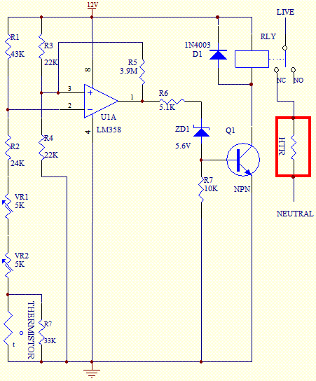
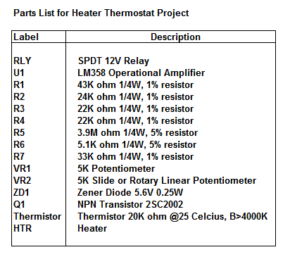
The circuit

The main part of Circuit is an amplifier. This sound signals (even at a distance of 2 meters from the mic) are picked up by the condenser microphone and converted into electrical variation, which are amplified by the op-amp. (Operational amplifier) IC- 741 is use in the inverting mode with a single supply using divider network of resistor the gain of IC can be set be varying the feed back through R5/6 resistance (can place a 1M variable) here the output of IC is further amplified buy the push-pull amplifier using transistor BC.548/558 pair, in this circuit are R2 is feed back resistance with R1/8 and C1/3 to connected IC-741. The IC’s pin 2 is connect VR1 (variable resistance) through connect to O/P of T1 (transistor) also use 6volt DC. The microphone should be placed near the circuit with the shield wire to suppress tune. The output of the amplifier is taken from emitter of two transistors, with a filter C5 from speaker. Same process continues in the second amplifier.

CIRCUIT DESCRIPTION OF SWITCH SECTION

This project was based on photo diodes and photo transistor. Photo diodes had been used as a transmitter and photo transistor as a receiver. This project had been divided in two part, First part transmitter section and second part receiver section. Slide switch selected to voice communication and data.

TRANSMISSIONSECTION :When switch key is pressed, circuit is energised. The output of The transmit IR beams modulated at same frequency 1KHz. The receiver uses infrared module. The IR- signal form the transmitter is sensed by the receiver sensor.

RECEIVER SECTION:- This section is worked as a Flip-flop (Bistable). IC-3 is decade counter, its Pin No.14 is input and Pin No. 2 output. The output of frequency detector stage is used, via a flip-flop, to switch ‘ON’ or switch ‘OFF’ a LED alternately. The receiver uses infrared modules IR-signal from the transmitter is sensed by the sensor through and its output PIN 1 goes low and switched LED. IC-3 is worked on clock pulse which receives to infrared modules at Pin No. 14. Its output at Pin No 2 throughes high.
The output of IC-2 is also used for lighting LED-1 indicating presence of signal. When no signal is available output of sensor module goes high and transistor LED is switched ‘OFF’. When another signal arrives, LED is switched ‘ON’ and through clock pulse at Pin No. 14 of IC-3. This makes the LED to switch ‘ON’ the appliance at first pulse and ‘OFF’ the appliance at its Second pulse arrived at its sensor. Transmitter circuits works satisfactorily with 6-9V DC. Battery but receiver circuits needs 6V regulated supply. The CAMD CM8870/70C provides full DTMF receiver capability by integrating both the band-split filter and digital decoder functions into a single 18-pin DIP, SOIC,or 20-pin PLCC package. The CM8870/70C is manufactured using state-of-the-art CMOS process technology for low power consumption (35mW, MAX) and precise data handling. The filter section uses a switched capacitor technique for both high and low group filters and dial tone rejection. The CM8870/70C decoder uses digital counting techniques for the detection and decoding of all 16 DTMF tone pairs into a 4-bit code. This DTMF receiver minimizes external component count by providing an on-chip differential input amplifier, clock generator, and a latched three-state interface bus. The on-chip clock generator requires only a low cost TV crystal or ceramic resonator as an external component.
Notes:
1. dBm = decibels above or below a reference power
of 1mW into a 600. load.
2. Digit sequence consists of all 16 DTMF tones.
3. Tone duration = 40ms. Tone pause = 40ms.
4. Nominal DTMF frequencies are used.
5. Both tones in the composite signal have
an equal amplitude.
6. Bandwidth limited (0 to 3KHz) Gaussian Noise.
7. The precise dial tone frequencies are
(350Hz and 440Hz) ±2%.
8. For an error rate of better than 1 in 10,000
9. Referenced to lowest level frequency component
in DTMF signal.
10. Minimum signal acceptance level is measured with
specified maximum frequency deviation.
11. Input pins defined as IN+, IN–, and TOE.
12. External voltage source used to bias VREF.
13. This parameter also applies to a third tone injected onto
the power supply.
14. Referenced to Figure 1. Input DTMF tone level
at –28dBm.
COMPONENTS USED

RESISTANCE:
R1, 150W
R2,R11,R12 100kW
R3, R7 10KW
R4, R8 4.7kW
R5,R6,R9,R10 15KW
R13 220K W
R14 1KW
R15-R22 150W
VR-1,VR-2 1MW Variable Resistance

CAPACITOR:
C1,C2,C4,C5 0.1 mfd (104 pf)
C3 220 mfd
MIKE Condensor Microphone

SEMICONDUCTOR:
IC1- UM91215B (DTMF CODER)
IC2, IC-3 741 (OP AMP)
IC-4 CM8870 (DTMF DECODER)
IC-5 74LS47 (DECODER)
T1,T3 NPN BC548
T2,T4 PNP BC558
LED Light Emitting Diode
Pt. Photo Transistor

MISCELLANEOUS:
IC Base 8 Pin (2pcs.)
Speaker 8 ohms
Optical Fibre General purpose
PCB General purpose
Slide Switch DPDT
Battery 6 volt DC

CIRCUIT DAIGRAM

RECEIVER

AUTOMATION SECTION

BLOCKDIAGRAM

CONSTRUCTION AND WORKING

IR-LED: It carries signals and converted into optical signals.

PHOTO TRANSISTOR: The electrical signals are regained from the optical signals.

DTMF CODER: It is generates the DTMF signal corresponding to the number entered from the keyboard.

DTMF RECEIVER/DECODER : It is fed to DTMF decoder which gives the binary output corresponding to the signal received from the transmitter.

DEMULTIPLEXER/ 4-16 LINE DECODER: It takes the 4 line BCD input and selects respective output one among the 16 output lines. It is active low output and drives to relay.

RELAY DRIVER : Its section controls the relay. It has a Not Gate and four NPN transistors. NPN transistor is drive to relay which works as a switching. Relay controls the AC devices.

WORKING OF AUTOMATION CONTROL SECTION:
Signal Decoding Unit:
This is the main unit of this system. This unit consists of a DTMF to BCD decoder IC MT 8870, 4 to 16 line decoder IC 74154 and hex inverter gate IC 4049. The working of all the above IC’s are mentioned here before.
The DTMF to BCD decoder IC MT8870 takes a valid tone signal from the IR transmitter section. Then the tone signal is converted in to 4 bit BCD number output obtained at pins from 11 to 14. This output is fed to the 4-16 line decoder IC74154. This IC takes the BCD number and decodes. According to that BCD number it selects the active low output line from 1 to 16 which is decimal equivalent of the BCD number present at its input pins. Since the low output of this IC the output is inverted to get logic high output. This inversion is carried out by hex inverter IC 4049- built on TTL logic. This IC inverts the data on its input terminal and gives inverted output.
3. Device switching unit:
This unit consists of a tri state buffer and a D flip flop. After making confirmation of current status of the device to alter the status of that device, you have to change the mode of the tri state buffer by making the control input high. This is done by pressing the ‘#’ key. When this key is pressed the output of the 4-16 line decoder goes low The output of tri state buffer is latched by using a D flip-flop. Here this D flip flop is used in the toggle mode. For each positive going edge of the clock pulse will trigger the flip-flop.
After a period of 5 seconds the output of the IC 6 goes low and puts the tri state buffer in the high impedance state. Therefore to change the status of any other device is to be done after the output of IC 6 goes low, again ‘#’ key is pressed to make the tri state buffer act as input –output state and the respective code of the device is pressed.
4. Power supply unit:
For the proper working of this local control section except the local telephone set it needs a permanent back up which gives a 5V back up continuously. This is achieved by using a 5V regulated power supply from a voltage regulated IC 7805. This 5V source is connected to all ICs and relays. This IC gets a backup from a 9V battery.
5. Relay driver circuit:
To carry out the switching of any devices we commonly use the relays. Since the output of the D flip flop is normally +5V or it is the voltage of logic high state. So we cannot use this output to run the device or appliances. Therefore here we use relays, which can handle a high voltage of 230V or more, and a high current in the rate of 10Amps to energize the electromagnetic coil of the relays +5V is sufficient. Here we use the transistors to energize the relay coil. The output of the D flip-flop is applied to the base of the transistor T2 – T5 via a resister. When the base voltage of the transistor is above 0.7V the emitter-base (EB) junction of the transistor forward biased as a result transistor goes to saturation region it is nothing but the switching ON the transistor. This intern switches on the relay. By this the devices is switches ON. When the output of D flip-flop goes low the base voltage drops below 0.7V as a result the robotic devices also switches OFF.
CIRCUIT DESCRIPTION:
This system is divided into two sections, 1: Remote Section 2: automation Control Section.
REMOTE SECTION:
This unit consists of IR transmitter section, which is present in the remote place. The figure (E) shows the circuit diagram of the DTMF encoder, which resembles the DTMF transmitter section. It uses DTMF encoder integrated circuit, Chip UM 91214B. This IC produces DTMF signals. It contains four row frequencies & three column frequencies. The pins of IC 91214 B from 12 to 14 produces high frequency column group and pins from 15 to 18 produces the low frequency row group. By pressing any key in the keyboard corresponding DTMF signal is available in its output pin at pin no.7. For producing the appropriate signals it is necessary that a crystal oscillator of 3.58MHz is connected across its pins 3 & 4 so that it makes a part of its internal oscillator.

Figure (E). Circuit diagram of the DTMF encoder

This encoder IC requires a voltage of 3V. For that IC is wired around 4.5V battery. And 3V backup Vcc for this IC is supplied by using 3.2v zener diode.
The row and column frequency of this IC is as on the fig. “B”. By pressing the number 5 in the key pad the output tone is produced which is the resultant of addition of two frequencies, at pin no. 13 & pin no.16 of the IC and respective tone which represents number ‘5′ in key pad is produced at pin no.7 of the IC. This signal is sent to the DTMF transmitter section through IR-LED.
ROBOTIC ARM CONTROL SECTION:
This is a control unit through which you can control your devices. This contains one DTMF transmitter section and a devices Control Section. The devices to be controlled must be connected to phototransistor through control unit. Control unit is kept with a sufficient backup.
devices control Section consists of a DTMF decoder, 4-16 line decoder/demultiplexer, D-flip-flops, and relay driver circuits. Before going into detail of the circuit, we will take a brief description about integrated circuits used in local control section.
MT 8870 DTMF decoder:
IC MT8870/KT3170 serves as DTMF. This IC takes DTMF signal coming via telephone line and converts that signal into respective BCD number. It uses same oscillator frequency used in the remote section so same crystal oscillator with frequency of 3.85M Hz is used in this IC.
Working of IC MT8870:
The MT-8870 is a full DTMF Receiver that integrates both band split filter and decoder functions into a single 18-pin DIP. Its filter section uses switched capacitor technology for both the high and low group filters and for dial tone rejection. Its decoder uses digital counting techniques to detect and decode all 16 DTMF tone pairs into a 4-bit code. External component count is minimized by provision of an on-chip differential input amplifier, clock generator, and latched tri-state interface bus. Minimal external components required include a low-cost 3.579545 MHz crystal, a timing resistor, and a timing capacitor. The MT-8870-02 can also inhibit the decoding of fourth column digits.
MT-8870 operating functions include a band split filter that separates the high and low tones of the received pair, and a digital decoder that verifies both the frequency and duration of the received tones before passing the resulting 4-bit code to the output bus.
The low and high group tones are separated by applying the dual-tone signal to the inputs of two 6th order switched capacitor band pass filters with bandwidths that correspond to the bands enclosing the low and high group tones.

Figure (F).Block diagram of IC MT8870

The filter also incorporates notches at 350 and 440 Hz, providing excellent dial tone rejection. Each filter output is followed by a single-order switched capacitor section that smoothes the signals prior to limiting. Signal limiting is performed by high gain comparators provided with by stresses to prevent detection of unwanted low-level signals and noise. The MT-8870 decoder uses a digital counting technique to determine the frequencies of the limited tones and to verify that they correspond to standard DTMF frequencies. When the detector recognizes the simultaneous presence of two valid tones (known as signal condition), it raises the Early Steering flag (ESt). Any subsequent loss of signal condition will cause ESt to fall. Before a decoded tone pair is registered, the receiver checks for valid signal duration (referred to as character- recognition-condition). This check is performed by an external RC time constant driven by ESt. A short delay to allow the output latch to settle, the delayed steering output flag (StD) goes high, signaling that a received tone pair has been registered. The contents of the output latch are made available on the 4-bit output bus by raising the three state control input (OE) to logic high. Inhibit mode is enabled by a logic high input to pin 5 (INH). It inhibits the detection of 1633 Hz.
The output code will remain the same as the previous detected code. On the M- 8870 models, this pin is tied to ground (logic low).
The input arrangement of the MT-8870 provides a differential input operational amplifier as well as a bias source (VREF) to bias the inputs at mid-rail. Provision is made for connection of a feedback resistor to the op-amp output (GS) for gain adjustment.
The internal clock circuit is completed with the addition of a standard 3.579545 MHz crystal.

74154 4-16 line decoder/demultiplexer:
IC 74154 is a 4-16 line decoder, it takes the 4 line BCD input and selects respective output one among the 16 output lines. It is active low output IC so when any output line is selected it is indicated by active low signal, rest of the output lines will remain active high. This 4-line-to-16-line decoder utilizes TTL circuitry to decode four binary-coded inputs into one of sixteen mutually exclusive outputs when both the strobe inputs, G1 and G2, are low. The demultiplexing function is performed by using the 4 input lines to address the output line, passing data from one of the strobe inputs with the other strobe input low. When either strobe input is high, all outputs are high. These demultiplexer are ideally suited for implementing high-performance memory decoders.

Figure G. IC 74154 4-16 line decoder
All inputs are buffered and input clamping diodes are provided to minimize transmission-line effects and thereby simplify system design.
TRUTH TABLE:

IC 4013 D-flip-flop:
IC 4013 is a conventional D-flip-flop IC. This IC consists of two D flip-flops. These flip-flops are used to latch the data that present at its input terminal. Each flip-flop has one data, one clock, one clear, one preset input terminals.

(Above figure shows a single D-flip-flop)

Relay driver circuit:
To carry out the switching of devices we commonly use the relays. Since the output of the D flip flop is normally +5V or it is the voltage of logic high state. So we cannot use this output to run the device or appliances. Therefore here we use relays, which can handle a high voltage of 230V or more, and a high current in the rate of 10Amps to energize the electromagnetic coil of the relays +5V is sufficient. Here we use the transistors to energize the relay coil. The output of the D flip-flop is applied to the base of the transistor T2 – T5 via a resister. When the base voltage of the transistor is above 0.7V the emitter-base (EB) junction of the transistor forward biased as a result transistor goes to saturation region it is nothing but the switching ON the transistor. This intern switches on the relay. By this the device is switches ON. When the output of D flip-flop goes low the base voltage drops below 0.7V as a result the device also switches OFF.
Power supply unit:
NEED OF POWER SUPPLY:-
Perhaps all of you are aware that a power supply is a primary requirement for the test bench of a home experimenter’s mini lab. A battery eliminator can eliminate or replace the batteries of solid-state electronic equipment and 220V A.C. mains instead of the batteries or dry cells thus can operate the equipment. Nowadays, the sued of commercial battery eliminator or power supply unit have become increasingly popular as power source for household appliances like transceiver, record player, clock etc.
Summary of power supply circuit features:-
Brief description of operation: gives out well regulated +8V output, output current capability of 500mA.
Circuit protection: Built –in overheating protection shuts down output when regulator IC gets too hot.
Circuit complexity: simple and easy to build.
Circuit performance: Stable +8V output voltage, reliable Operation.
Availability of components: Easy to get, uses only common basic components.
Design testing: Based on datasheet example circuit, I have used this circuit successfully as part of other electronics projects.
Applications: part of electronics devices, small laboratory power supply.
Power supply voltage: unregulated 8-18V-power supply.
Power supply current: needed output current 500 mA.

Components cost: Few rupees for the electronic components plus the cost of input transformer.

Pin Diagram of 7808 Regulator IC
Pin 1: Unregulated voltage input
Pin 2: Ground
Pin3: Regulated voltage output

Component list

7808 regulator IC
2. 0-12 transformer
3. 1000uf and 100uf. Capacitor, at least 25V voltage rating.
DESCRITION OF POWER SUPPLY

This circuit is a small + 8 volts power supply. Which is useful when experimenting with digital electronics. Small inexpensive battery with variable output voltage are available, but usually their voltage regulation is very poor, which makes them not very usable for digital circuit experimenter unless a better regulation can be achieved in some way. The following circuit is the answer to the problem.
This circuit can give +8V output at about 500mA current. The circuit has overload and terminal protection.

CIRCUIT DIAGRAM OF POWER SUPPLY
The above circuit utilizes the voltage regulator IC 7808 and 7805 for the constant power supply. The capacitors must have enough high voltage rating to safely handle the input voltage feed to circuit. The circuit is very easy to build for example into a piece of Zero board.
For the proper working of this local control section except the mobile phone or local telephone set it needs a permanent back up which gives a 8V back up continuously. This is achieved by using a 8V regulated power supply from a voltage regulated IC 7808. This 5V source is connected to all ICs and relays. This IC gets a backup from a 9V battery.

Fig J. Circuit Diagram of Local Control Section.
USED COMPONENTS

SEMICONDUCTORS
(1) IC-1 ……… 7808
(2) IC-2…………. CM8870P
(3) IC-3…………. 74154
(4) IC-5-6………CD 4013
(5) IC-4……….. 4049
(6) IC7 ………… UM 91214B
(7) D1-D2 ………….IN 4007
(8) D3…………… 3V Zener
(9) LED ……………. Light Eammiting Diode
(10) T1-T6…………..(NPN) 368
(11) Crystal ………… 3.57 Mhz.
(12) Photodiode
(13) Phototransistor

RESISTOR
(1) R1……….330K OHm.
(2) R2……….. 100K OHm.
(3) R3,R4,R7 ………. 10K OHm.
(4) R5,R6, ………. 1K OHm.
(5) R8-R12…. 100 OHm.

CAPACITOR
(1) C1…………. 1000MFD.
(2) C2,C3…………. 0.1 MFD.

MISCELLANEOUS
(1) RELAY ………………. 6V \100 0Hm.
(2) TRANSFORMER…… 0-9 (Step down)

Vehicle Monitoring and Security System (latest)

ABSTRACT: In this modern, fast moving and insecure world, it is become a basic necessity to be aware of one’s safety. Maximum risks occur in situations wherein an employee travels for money transactions. Also the Company to which he belongs should be aware if there is some problem. What if the person traveling can be tracked and also secured in the case of an emergency?! Fantastic, isn’t it? Of course it is and here’s a system that functions as a tracking and a security system. It’s the VMSS. This system can deal with both pace and security.

The VMSS (Vehicle Monitoring and Security System) is a GPS based vehicle tracking system that is used for security applications as well. The project uses two main underlying concepts. These are GPS (Global Positioning System) and GSM (Global System for Mobile Communication). The main application of this system in this context is tracking the vehicle to which the GPS is connected, giving the information about its position whenever required and for the security of each person travelling by the vehicle. This is done with the help of the GPS satellite and the GPS module attached to the vehicle which needs to be tracked. The GPS antenna present in the GPS module receives the information from the GPS satellite in NMEA (National Marine Electronics Association) format and thus it reveals the position information. This information got from the GPS antenna has to be sent to the Base station wherein it is decoded. For this we use GSM module which has an antenna too. Thus we have at the Base station; the complete data about the vehicle.

Along with tracking the vehicle, the system is used for security applications as well. Each passenger/employee will have an ID of their own and will be using a remote containing key for Entry, Exit and Panic. The Panic button is used by the driver or the passenger so as to alert the concerned of emergency conditions. On pressing this button, an alarm will be activated which will help the passenger/employee in emergencies and keep them secure throughout the journey. The vehicle can also be immobilized remotely.

INTRODUCTION:

Of all the applications of GPS, Vehicle tracking and navigational systems have brought this technology to the day-to-day life of the common man. Today GPS fitted cars, ambulances, fleets and police vehicles are common sights on the roads of developed countries. Known by many names such as Automatic Vehicle Locating System (AVLS), Vehicle Tracking and Information System (VTIS), Mobile Asset Management System (MAMS), these systems offer an effective tool for improving the operational efficiency and utilization of the vehicles.

GPS is used in the vehicles for both tracking and navigation. Tracking systems enable a base station to keep track of the vehicles without the intervention of the driver whereas navigation system helps the driver to reach the destination. Whether navigation system or tracking system, the architecture is more or less similar. The navigation system will have convenient, usually a graphic display for the driver which is not needed for the tracking system. Vehicle tracking systems combine a number of well-developed technologies.

To design the VMSS system, we combined the GPS’s ability to pin-point location along with the ability of the Global System for Mobile Communications (GSM) to communicate with a control center in a wireless fashion. The system includes GPS-GSM modules and a base station called the control center.

Let us briefly explain how VMSS works. In order to monitor the vehicle, it is equipped with a GPS-GSM VMSS system. It receives GPS signals from satellites, computes the location information, and then sends it to the control center. With the vehicle location information, the control center displays all of the vehicle positions on an electronic map in order to easily monitor and control their routes. Besides tracking control, the control center can also maintain wireless communication with the GPS units to provide other services such as alarms, status control, and system updates.

The design takes into consideration important factors regarding both position and data communication. Thus, the project integrates location determination (GPS) and cellular (GSM) – two distinct and powerful technologies in a single system.

VMSS is based on a PIC microcontroller-based system equipped with a GPS receiver and a GSM Module operating in the 900 MHz band. We housed the parts in one small plastic unit, which was then mounted on the vehicle and connected to GPS and GSM antennas. The position, identity, heading, and speed are transmitted either automatically at user-defined time intervals or when a certain event occurs with an assigned message (e.g.; accident, alert, or leaving/entering an admissible geographical area).

The GPS Module outputs the vehicle location information such as longitude, latitude, direction, and Greenwich Time every five minutes. The GSM wireless communications function is based on a GSM network established in a valid region and with a valid service provider. Via the SMS provided by the GSM network, the location information and the status of the GPS-GSM VMSS are sent to the control center. Meanwhile, the VMSS receives the control information from the control center via the same SMS. Next, the GPS-GSM VMSS sends the information stored in the microcontroller via an RS-232 interface.

There are two ways to use the VMSS’ alarm function, which can be signified by either a buzzer or presented on LCD. The first way is to receive the command from the control center; second way is to manually send the alarm information to the control center with the push of a button.

The base station consists of landline modem(s) and GIS workstation. The information about the vehicle is received at a base station and is then displayed on a PC based map. Vehicle information can be viewed on electronic maps via the Internet or specialized software. Geographic Information Systems (GIS) provides a current, spatial, visual representation of transit operations. It is a special type of computerized database management system in which geographic databases are related to one via a common set of location coordinates.

STAGES OF VMSS

STAGE 1:
Driver starts his trip from the transport office.
VMSS transmits the Driver I.D and the Vehicle I.D along with the position of the vehicle to the base station.

STAGE 2:
Taxi picks up the employee/passenger from their residence.
VMSS transmits the Passenger I.D and the Vehicle I.D along with the position of the vehicle to the base station. Therefore base station will be able to keep a track of the vehicle and thus the employee/passenger.

STAGE 3:
Taxi drops the employee/passenger to the workplace.
VMSS transmits the Passenger I.D and the Vehicle I.D along with the position of the vehicle to the base station.
STAGE 4:
Taxi picks the employee/passenger from the workplace.
VMSS transmits the Passenger I.D and the Vehicle I.D along with the position of the vehicle to the base station. Therefore this enables the base station to estimate the time if required and also keep a track of the vehicle, passenger and the driver.