We can control any electrical device in homes and businesses with the Internet of Things (IOT). Additionally, from anywhere in the globe, you may read data from any sensor and visually analyse it. Using an Arduino Uno and an ESP8266-01 module, we can read the temperature and humidity data from the DHT11 sensor and upload it to a ThingSpeak cloud. The Arduino Uno is an MCU that receives temperature and humidity data from a DHT11 sensor, processes it, and sends it to an ESP8266 module. One of the top platforms for the Internet of Things is the WiFi module known as ESP8266. It can send a data packet to the IOT cloud.
Popular Posts
-
RESEQUENCING ANALYSIS OF STOP-AND-WAIT ARQ FOR PARALLEL MULTICHANNEL COMMUNICATIONS:--DOTNET--2009 RESEQUENCING ANALYSIS OF STOP-AND-WAIT AR...
-
Introduction This amplifier does not claim to be "state of the art", and in fact the base design is now over 20 years old. It is ...
-
Signals, including those used for communication between occupants of a car or train.Indicators, recorders, telegraphic, telephonic, or oth...
Saturday, 25 June 2022
Arduino Uno-based IoT Humidity and Temperature Monitoring
Monday, 9 April 2012
Heat Control System
Introduction
This project was the first stage of developing a controller for a radiant floor heat system. The microcontroller will use inputs from thermostats, thermocouples, a flow meter, and pressure switches to control the operation of the pumps and valves to achieve improved efficiency of the system as a whole.
This project idea came from a friend who recently built a house which utilizes an outdoor wood boiler for heating. He expressed that he was disappointed in the efficiency of the current system and wished he had more control over the system operation. This seemed like a good application of what I�ve learned in this course. The main goal is to improve the efficiency of the system by shortening the amount of time that the Pumps need to run while still properly heating the home. By doing this, consumption of both electricity and wood will be reduced.
Implementation of this project involves a large amount of work outside of the microprocessor. Because of this, I bound the scope of this academic project to the control logic only. In order to implement this in the house, I will have to build the circuitry to translate the control logic over to the voltages necessary for operation of the valves, pumps and sensors. In order to verify and validate the controller logic worked as desired I built a demonstration board that models the inputs and outputs of the system. This board was used to debug the controls during development and it was also a convenient way of demonstrating this project at the end of the semester. Toggle switches were used to model the 5 thermostats, adjustable voltage dividers were used for thermocouples, a 555 Timer circuit was used for the flow meter and LEDs were used for all outputs.
Friday, 2 December 2011
Smart Fan: A Human Tracking Fan System
The two PIR sensors are separated in the middle. The purpose of this is to separate the sensors’ field of view.
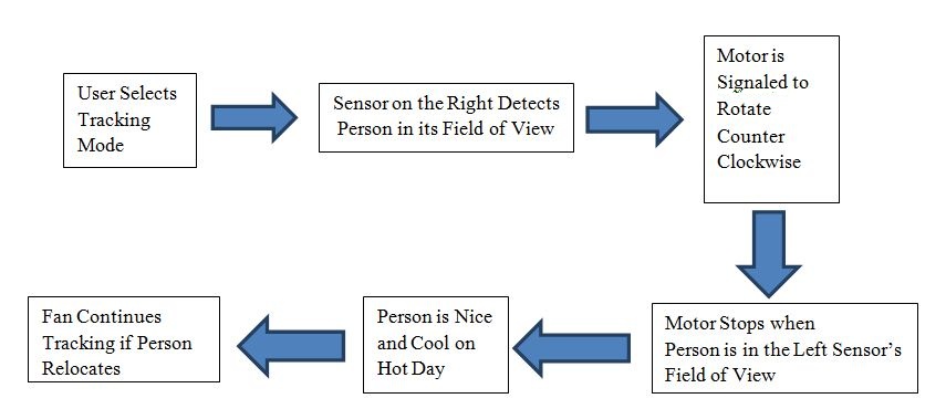
When a sensor detects the right amount of infra-red light a comparator output goes high. We use the microcontroller to generate an interrupt on the comparator’s rising edge. The interrupt then signals a task that begins rotating the platform’s motor. The rotation is clockwise if the left sensor has detected a person or counter clockwise if the right sensor has detected a person. Once the fan is directed at the person’s location, there is just enough infra-red light in the second sensor’s field of view to trigger its comparator. This generates an interrupt that signals a task to either stop or redirect the motor, depending on the setting. At this point the customer is nice and cool without exerting any effort.
An example of the fan’s operation is illustrated in the block diagram below.
LED-Following Car
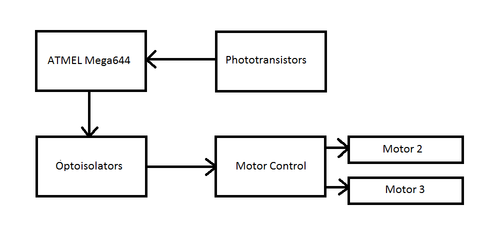
In our project, the phototransistors sent their outputs to the ATMEL Mega644 microcontroller. The MCU then calculates which motors should move based on the phototransistors and sends a signal to the optoisolators telling which motors to turn on. Depending on which optoisolator is turned on, the motor control will tell which motor to move. We used optoisolators to separate the MCU from the motor circuitry. Optoisolators isolate the LED side of the circuit from the phototransistor side of the circuit, ideally protecting the MCU from any unknown outputs from the motor controller.
Friday, 27 May 2011
Simple Alarm System
The circuit presented here is a very simple and yet highly effective alarm system for protecting an object. The circuit requires no special devices and can be built using components that you will no doubt be able to find in the junk box. The alarm-triggering element is a simple reed switch. To generate the alarm signal itself any optical or acoustic device that operates on 12 V can be used: for example a revolving light, a siren, or even both. In the quiescent state the reed switch is closed. As soon as the reed switch opens, the input to IC1.B will go low (previously the potential divider formed by R2 and R3 held the input at 5.17 V, a logic high level).

A turn-on delay of between 0 and approximately 90 s can be set using P1, and a turn-off delay of between 0 and approximately 20 s can be set using P2. When the system is turned on (using S1), the turn-on delay is activated, giving the user of the system at most 90 s to leave the object alone before the system goes into the armed state, and the object is then protected. Once the reed switch opens the turn-off delay of at most 20 s starts: this allows the rightful owner of the object to turn the system off before the alarm is triggered. If some unauthorised person causes the reed switch to open, the alarm will be triggered after the turn-off delay.

Also, even if the reed switch is briefly opened and then closed again, the alarm will still be triggered. Once the alarm is triggered, T3 will conduct for about 45 s (because of R8 and C5). The turning off of the alarm is necessary to avoid the nuisance caused by a permanently sounding alarm system. The system then returns to the armed state, which means that the next time the reed switch is opened the alarm will trigger again. If it is not desired that the duration of the alarm be limited, for example if a visual indication is used, D5 should not be ?tted. The system can be extended by ?tting multiple reed switches in series. As soon as any one is opened, the alarm is triggered.

When S1 is closed C3 charges via P1. Depending on the potentiometer setting, it takes between 0 and 90 s to reach the input threshold voltage of IC1.A. The output of IC1.A then goes low and D3 stops conducting. Assuming the reed switch is closed, the inputs of IC1.B stay high and the output therefore low. If the reed switch is opened after the turn-on delay expires the output of the gate will change state and turn on T1. This ensures that the output of the gate remains high even after the reed switch is closed again. C4 now starts charging via P2, reaching the input threshold voltage of IC1.C after between 0 and 20 s, again according to the potentiometer setting. The output of IC1.C goes low, and T2 and T3 are turned on – and the siren sounds.
Any Darlington transistor can be used for T3. At the same time, C5 charges via R8, reaching the input threshold of IC1.D in about 45 s. When the output of IC1.D swings low, it pulls the inputs of IC1.A low via diode D5: the siren stops and the system returns to the armed state. If the potentiometers P1 and P2 are replaced by ?xed resistors it is possible to build the circuit small enough to ?t in a match-box, without the need to resort to SMD components. This is ideal if the circuit is to be used to protect a motorbike. If the alarm system is to be used in a car, an existing door switch contact can be used instead of the reed switch. In this case an RC combination needs to be added to prevent false triggering. Use a 10 µF/25 V electrolytic for C6, a 100 k? resistor for R9 and a 1N4001 for D7. It is again possible to wire multiple door switch contacts in parallel: as soon as one contact closes, IC1.B will be triggered.
Thursday, 27 January 2011
Zigbee Wireless Relay Control and Power Monitoring
What this group is working on is an energy-monitoring system for a home using alternative energy sources. A very high-level block diagram of this system is shown below:

Figure 1. High-level diagram of the "Smart Home Energy Monitoring System."
In the above diagram, the “Magic Box” essentially exists to route energy between the house, the various energy sources (for example, a solar cell or the electric grid), and an energy storage unit (such as a rechargeable battery). In this project, we will “black box” this Magic-Box system, and instead focus on another portion of this energy monitoring system, which involves sending data regarding energy usage and various energy loads (by wirelessly controlled relays) to a PC in order to display and monitor energy usage within the home.
· Our project focuses on the House to In-Home Display (IHD) part of this system. What our project does is the following:
· Simulates a home by using resistors to model various appliances or groups of appliances
· Allows a user to wirelessly turn on and off various sets of appliances by controlling relays
· Monitors total power consumption and current in this home
· Wirelessly transmits the above data to a PC, displaying the data on a graph that shows real-time power consumption in the home (or simulated home)
Our simulated “home” consists of 7 appliances, each modeled by a resistance (a load). These 7 loads are all in parallel, and are fed voltage from a 5 V DC source (the microcontroller). In a real house, the source voltage would be 120 V AC (in the United States at least). We considered attempting to implement this, but considering the practical dangers of “playing around” with 120 V AC circuits as well as the fact that a relay control system shouldn’t depend on the voltages being fed through the relays led us to decide to stick with 5 V DC circuits for testing and simulation.
Background Theory
What we have built is a simple transmission system based on the Zigbee routing and networking protocol. This protocol and its details are discussed in greater detail in the Standards section (below); in this section, we focus on underlying network theory and the role this theory played in our project.
Data networks (and transmission systems) are typically divided into various layers based on functionality. This is sometimes called a “protocol stack” (in our case, we are using a “Zigbee stack”). Essentially, the lower the layer, the closer we are to worrying about actual physical electrons flying around. Conversely, the higher the layer, the less we are worrying about physical constraints and the more abstract the data structures are that we are dealing with and manipulating.
The most famous of these layering models is the Open System Interconnection (OSI) Reference Model, which is shown below:
Figure 2. The OSI Reference Model (Source: http://en.wikipedia.org/wiki/OSI_model)
The functionality of each layer (or group of layers) is described in a bit more detail below.
Physical Layer
The physical layer's job is to move individual digital bits from one place to another. The protocols in this layer depend on the actual physical medium. For example, in a wireless system, the actual physical medium is simply the atmosphere.
Link Layer
A network's link layer routes a series of bits (sometimes called a datagram) from one node in a network to another. This can happen through a series of intermediate switches (or routers). Protocols at this layer provide more robust and full-featured services than protocols at the physical layer. WiFi is one example of a link-layer protocol.
Network and Transport Layers
Again, since these layers are higher in the model, protocols at this layer typically are more full-featured than protocols at the link or physical layers. Protocols at these layers use the link layer's routing capabilities to move the aforementioned datagrams between nodes in a network. The Internet Protocol (IP) is probably the most famous network layer protocol, while the Transmission Control Protocol (TCP) and the User Datagram Protocol (UDP) are two examples of well-known and widely-used transport-layer protocols. Certain higher-level functionality is more prevalent in these two layers than in lower levels. For example, flow control – controlling the transmission rate between nodes in order to lower congestion on the network (realizing that even just a two-node transmission system can be considered a “network”) – and reliable transmission (ensuring that a packet is actually received) are two features commonly implemented in the network and transport layers.
Session, Presentation, and Application Layers
These layers are essentially the end-result of a networking protocol stack. For example, a web browser resides in the application layer. These layers make use of all of the lower layers to send data between nodes on a network, and then use their own protocols for manipulating that data. A web browser renders HTML but uses lower-level protocols to send HTML between nodes in a network.
Our Project
The part of our project that we implemented basically deals with the network layer and above. The XBee chips (which are discussed in much greater detail later in the report) and firmware allow us to “black box” the Data Link and Physical layers, and the open source Xbee-API and Xbee-Arduino software packages greatly simplified our work in the network layer. Thus, it was not strictly necessary for us to have a deep understanding of the underlying physical, link, and network layer protocols used, but a brief discussion of this is warranted nonetheless.
The physical layer protocol/standard used in Zigbee systems is IEEE 802.15.4 (http://www.ieee802.org/15/pub/TG4.html). This is a wireless standard that operates, in North America, in the range of 2400-2483.5 MHz or 902-928 MHz. Zigbee, and most importantly our chips, operate in the higher 2.4 GHz range, so that is the range we will briefly discuss here. The data transmission rate is up to 250 kilobits per second.
Logical Structure
A block diagram of our system is shown below. As you can see there are seven relays which are controlled by the MCU. The MCU gets its command from the Xbee Chip which is wirelessly transmitted from another Xbee chip that is connected to the PC. The user can specify from the PC which relays they want to turn on and off. Also all seven of the relays load goes through a .2 ohm power resistor which goes through an optoisolator to keep it safe from the MCU and finally to the Xbee chip. This gets transmitted back to the PC to be displayed on a graph in a GUI.

Saturday, 13 November 2010
Audio based Navigtor
Navigation in the past has primarily relied on the use of a map, compass or other devices that must be interpreted visually. This project demonstrates the ability to navigate a user based on synthesized directional audio which allows the user to move to a known location without the use of a visual aid. The module uses a GPS, a digital compass, and an ATmega32 to generate sound based on the direction that the user must turn in order to face the correct direction.
Sound Byte
The goal of this project was to create a device that allows a user to navigate to a predefined location though the use of auditory guidance.
The module uses GPS and a digital compass to determine at what angle the user hears the sound pulses. On initial startup the user selects from a number of predefined locations through the use of an LCD screen. Once the GPS has a lock, the module determines the bearing (angle from true North) that the user must travel to get to the destination. This angle is compared with the compass output and a sound is made based on which direction the user must turn to face the final location. The sound consists of short pulses that are delayed between the right and left side and modulated in amplitude to give the effect of direction.
One example implementation of this is self guided tours. A user could be guided though a predetermined course by following the sound of a recorded person's voice. In such a setting, if the user were to veer off course, the system would guide then guide the user back on course. Also, the direction of the guide's voice could be used to highlight the object of interest along the tour.
The project idea came after Dr. Land mentioned that you could create the effect of a sound coming from a location by properly spacing the left and right channel by a certain distance. It seemed like a good idea to use this for navigation. This principle is based in the way that humans naturally hear perceive direction. Sound will reach each ear at a slightly different time and volume. Based on those differences, humans are able to determine the direction of sound in the horizontal plane.
Figure 1 shows the high level design of system.
Figure 1: High level system design
The GPS communication uses a standard format (NMEA0283 V 2.2). These standards include GGA, GSV, GSA, and RMC. Of these, RMC (Recommended Minimum Navigation Information) is used in the final product for simplicity. Useful information from this protocol includes time, status, latitude, longitude, speed, and date. The other standards were used for development and debugging.
At this time there is no knowledge of existing patents, copyrights, and or trademarks that are relevant to this project. There are many devices that utilize GPS or a compass, but not together with this synthesized audio.
Having three group members made it nice as there were three distinct portions to the project, GPS, compass, and the synthesized audio. Each portion was developed on its own while keeping the others in mind and brought together at the end. For example, planning for the project included allocating resources between the sub functions including timers, registers, and ports.
Bringing together the three separate parts was tricky because of the timing budget. It was known that the GPS could only refresh at 1 Hz, but the sound and compass must be run much faster. We wanted the sound direction to change smoothly during the course of turning your head (faster than 1 Hz). Therefore, the GPS was allowed to run as fast as it could, depending on how many satellites were locked, and how many sound and compass functions were packed in between. This became tricky when multiple satellites were locked and the data stream from the GPS is continuous. The main structure of the program can be seen in Figure 2.
Figure 2: Software flow chart
The digital compass module used was a Hitachi HM55B from Parallax, mainly because we already had it before the project. The communication between this device was done with three wires (clock, data, and enable) in an SPI like fashion. The communication is based on the Basic Stamp function SHIFTIN/SHIFTOUT which is a two wire communication. The challenge was to implement this in C for the ATmega32. Timer1 was used to control the timing of the function and three GPIOs were used for the three controls. The compare interrupt was used to generate the clock and data as this allowed for the clock time to be set at fine resolution resulting in the fastest possible operation of the compass. The clock signal was generated at twice the data rate so that data could be clocked on both the rising and falling edge of the clock in attempt to keep this function as general as possible in case of future use for other projects. To get data, the ATmega32 pulses the enable bit high for two clock cycles, then sends 0b0000 on the shared data_in and data_out line. After another enable toggle, 0b1000 gets sent to the compass signifying a start measurement command. The ATmega32 then sends 0b1100 and reads in four bits waiting for the data conversion to be done. When the compass sends back 0b1100, the data is ready. The ATmega32 then clocks in 22 bits (11 for x value, and 11 for y value) of 2s complement data MSB first. After properly formatting the data to get the proper sign an atan(x/-y) is called to result in an angle. This is then converted from radian to degrees and compensated for the difference between true and magnetic North (subtracting 12 degrees here in Ithaca). The whole function takes 60mS to run, which was determined to be fast enough.
The PWMs from timers 0 and 2 are used to generate sound pulses. Each timer is set to operate in fast PWM mode with a prescaler of one, giving the PWMs a sample rate of 62500 sample/second. The overflow interrupts of each timer are used to update the OCR.
Initially, timer1 of the Atmega644 was used to generate two PWM waveforms. The idea was that since timer1 has two output compare registers, it should be able to generate two PWMs. Timer1 was able to generate two PWMs, but since OCR1A was used as the top value and the PWM waveforms were not unique, the outputs of OCR1A and OCR1B toggled whenever the overflow interrupt was triggered. Using two timers prevented the overflow interrupt from toggling both pulses and also allowed for one timer to be used as a time based when an interrupt was triggered.
The code used for direct digital synthesis was adopted from lab2 written by Dr. Land4. The DDS process consists of a sin function quantized into a 256 entry table and a ramp table to linearly increase or decrease wave amplitude. For this project, two more tables were used to represent the phase offset and amplitude of the wave at a given source degree. These tables are precomputed to prevent extra computation during execution.
The premise of delaying sounds arriving at each ear to simulate sound localization is based upon interaural time difference. By delaying the sound arriving at one ear by up to 660 microseconds, the sound will have the appearance of coming from the side of the leading sound pulse.5 For example, if the channel going to the left ear is delayed, then the listener will interpret the delay as a sound source that is closer to the person's right ear.
The phase offset table is used to represent the delay that is present at each degree. It was constructed to achieve no offset at a zero degree heading (the source is directly in front of the user) and maximum offset at 90 or 270 degrees. If the sound source is behind the user, then the channel of the ear furthest from the source will be fully delayed, encouraging the user to turn his or her head to better discriminate the location of the sound.
To make the sound direction more apparent, the amplitude of the delayed channel is also reduced. The sound is scaled according to a normal distribution so that full intensity is delivered when the user faces the source with a zero degree difference. As the user rotates away from the source direction, the amplitude of the PWM wave channel furthest from the source is reduced while the closer channel maintains full intensity.
We used interrupt driven serial communication over the USART to receive data from the GPS. The GPS outputs NMEA sentences approximately once a second at 4800 baud. An example of one packet of NMEA sentences is shown below.
$GPGGA,144739,4251.9960,N,07806.0827,W,1,04,5.6,1898.0,M,34.5,M,,*61
$GPRMC,144739,A,4251.9960,N,07806.0827,W,1908.5,270.0,050510,5,E,A*2F
$GPGSV,8,1,32,01,12,205,-18,02,43,251,14,03,08,022,-22,04,05,271,00*75
$GPGSV,8,2,32,05,78,032,45,06,83,236,48,07,81,084,47,08,64,206,33*71
$GPGSV,8,3,32,09,90,086,52,10,42,202,13,11,26,284,-4,12,88,117,51*6C
$GPGSV,8,4,32,13,90,027,52,14,68,030,37,15,78,143,44,16,60,220,30*7E
There are several cases of redundant data between NMEA sentences and, for the purposes of this project; we only need one set of longitude and latitude. We decided to only read in the RMC (Recommended Minimum Content) sentence as a string and then extract the longitude and latitude from that string.
We use the USART character-ready interrupt which triggers as soon as a full character is received by the USART buffer. Once a character is ready in the USART buffer, the ISR writes the character to a string buffer and enters the state machine. The state machine successively checks for the characters that are expected to be seen at the beginning of the RMC sentence. If the program does not receive the expected header characters, it returns to the beginning of the state machine. If the input characters are ‘$’,’G’,’P’,’R’,’M’, and ’C’ in succession, program records the rest of the sentence as data. The sentence is terminated with the ‘\n’ character.
The data from the RMC sentence is written to a string buffer. Knowing the format of the RMC sentence, we use sscanf to extract the longitude and latitude. The longitude and latitude are sent in the format DDMM.MMMM where DD is in degrees and MM.MMMM is in seconds. We parse the data and recalculate the values in terms of degrees. It should also be noted that when writing to the string buffer, we ignored decimal points due to difficulties with sscanf reading in floating point numbers on the microcontroller. In order to compensate for this, we scaled the longitude and latitudes appropriately during the conversion into degrees and then radians.
We use the following equation to calculate the direction from the user’s current location to the final destination:
atan2(sin(dlon)*cos(lat2), (cos(lat1)*sin(lat2))-(sin(lat1)*cos(lat2)*cos(dlon)));6
where lat1=current latitude, lat2=target latitude, and dlon=difference in current and target longitude.
System Integration/Timing
In order for the interrupts to run at their desired speeds, we found that it was necessary that they not run at the same time. For this reason, we timed our system to first receive data from the GPS, and then run the compass data retrieval function and sound output as many times as possible before the next packet from the GPS.
We start the timing on the first packet received from the GPS and let the USART interrupt run until the entire RMC sentence is received. Once the RMC sentence is received, we turn off the USART interrupt in order to not interrupt on all of the characters of the other NMEA sentences. We then enable the interrupts for the compass function which takes approximately 60ms. As soon as the compass function ends, the sound function and its interrupts are run. The sound function will vary in length
based on its output, but it should never take more the 150ms. We then repeat the compass and sound functions again before turning the USART interrupt on, which will wait for the next RMC sentence. Running the compass and sound functions twice leaves enough time for the USART to be enabled before the next RMC sentence arrives.
The supporting hardware consisted of two active low pass filters used to buffer the audio. The wire routing was kept as compact as possible meaning that data lines ran close to the audio introducing a lot of noise. Using a custom PCB could remedy the problem, but was out of the scope of this project. A potentiometer was used on each channel to adjust the volume allowing ensuring equal volumes when pointing at the destination. Also, an LCD screen was used to select the initial destination. This was done with three buttons, screen up, screen down, and select. These were implemented active low with a 10k ohm pull up resistor and a 330 ohm resistor current protection.
It was found that overall the device worked as expected as multiple users were able to direct themselves to a location that they were unaware of. The rate at which the GPS acquires data is at best once a second and depends on the number of satellites locked. The sound and compass update twice a second. This is a little slower than desired, but is limited by the speed of the GPS and the computations of the bearing value. Three sound pulses might be possible if the math for the GPS (shown above) is changed from floating point to fixed point. A picture of the final device can be seen in Figure 3. LCD screen is located on the top of the device. This means that the user must take the device off to change location. This is acceptable as a compact unit was part of the project description.
Figure 3: Final Device
The accuracy of the device was found to be subjective to the user and their ability to recognize small differences in the sound pulses. However, it was found that in general the average user was able to resolve a direction to within +/- 10 degrees. The locations for the different data points were initially found with the use of a Motorola Droid and its internal GPS. This was found to be very accurate and provided a location to within a 3 meter radius.
Safety was not a big concern throughout the project, other than being alert and keeping your eyes open when navigating to the final destination. The project did not interface with other projects in a negative way, other than the occasional noise made while testing. The final project is a self contained unit that does not interfere with anything else.
This device could be used to solve a number of issues. As mentioned before, one could be used for self guided tours. Also, a boat operator might find it useful when navigating a boat at night time for far distance navigation. It can be understood that this would be useful for anyone needing navigation while not being able to look at a map. This could be useful for orienteering as you would not need to look at a map but could focus on the environment around you
Our initial goal was to guide a person by sound using data gathered from a GPS module. Before we started our project we acknowledged that the GPS module would have some uncertainty and there would be difficulty determining if the person was directly over the target location. Given the budget of this project we decided to sacrifice GPS accuracy in favor of staying within budget.
Our final prototype not only stayed within budget, but the GPS module performed to our expectations and the directional sound was sufficiently accurate. During the demo for this project, the professor, Dr. Land, was able to follow the sound pulses to a location about 5 minutes walking distance away. Dr. Land had no previous training with this device, but he was able to final the target location within 3 meters. Other curious bystanders were also able to identify the direction of target with very little direction.
If this project were to be improved, then a different GPS module capable of updating at 5Hz could be used instead of the 1Hz GPS used in the current prototype. This would increase the budget by about $25, but the code would also have to be altered to accommodate the more frequent updates. However more updates would require a faster clock speed, less frequent PWM pulses, or both. A different compass with a higher resolution than 6bits could also be used, but this would also increase the price of the project.
As mentioned in the introduction the GPS communication uses a standard format (NMEA0283 V 2.2). These standards include GGA, GSV, GSA, and RMC. Of these, RMC (Recommended Minimum Navigation Information) is used in the final product for simplicity. The other standards were used for development and debugging.
The code that was adapted from the 4760 website was from lab 2. This code consisted of using the PWM for DDS.
Intellectual property considerations:
This project was designed to aid a person in guiding them towards a destination. It is not intended to be used to assist a person purely based upon sound. The navigation data used by this device is based upon GPS data, therefore obstacles are not taken into consideration and this device will not guide a person around any potential hazards.
The device does not produce an electrical shock or any other hazard that may cause harm to the person wearing it. The device is powered by a household 9V battery, therefore all safety considerations that apply to the proper handling of 9V batteries also apply to this device. The bread board is insulated from the user by the headphones. The only safety consideration that may affect the individual wearing this device is if the person wears it in the rain. Although the device is insulated from the user's head, the device does not have a cover to prevent moisture damage. Therefore this device should not be worn in any circumstance where it could be contaminated by moisture.
The data gathered by the GPS is only stored long enough to determine the direction that the user must travel. The data is not stored or tracked by any other means. Therefore, the privacy of the user is not violated by tracking the location of user.
Task List
Nick - GPS, Audio buffering/Filtering, general debug
Matt - Sound (PWM), LCD/Buttons, general debug
Garret -Compass, Combined three main programs together
Compass Module - http://www.parallax.com/Store/Microcontrollers/BASICStampModules/tabid/134/ProductID/98/List/1/Default.aspx?SortField=UnitCost,ProductName
GPS Module - http://www.parallax.com/StoreSearchResults/tabid/768/txtSearch/GPS/List/0/SortField/4/ProductID/560/Default.aspx
ATmega 32 - http://www.parallax.com/StoreSearchResults/tabid/768/txtSearch/GPS/List/0/SortField/4/ProductID/560/Default.aspx
ECE4760 - http://instruct1.cit.cornell.edu/courses/ee476/
Interaul Time Difference- http://en.wikipedia.org/wiki/Interaural_time_difference
http://www.movable-type.co.uk/scripts/latlong.html
In order to make the sound more pleasing to the ear and not nauseating, we had to keep the pulses consistently spaced in a consistent pattern. We did this by timing how long each function took and then spacing them out based on this. We initially tried to run the compass and sound one by one while the USART was running in the background the entire time. The overlapping interrupts caused unpredictable delays which were not only nauseating, but caused the data updates to be too slow for reasonable use.
Tuesday, 20 July 2010
Blood Pressure Monitor Block Diagram and Design Considerations
Design Considerations:
Blood pressure monitors can use Korotkoff, Oscillometry, or Pulse Transit Time methods to measure blood pressure. They employ a pressure cuff, pump, and transducer to measure the blood pressure and heart rate in three phases: Inflation, Measurement, and Deflation. They include an LCD, memory recall, selection buttons, power management, and USB interface.
The pressure transducer produces the output voltage proportional to the applied differential input pressure. The output voltages of the pressure transducer range from 0 to 40 mV, which needs to be amplified so that the output voltage of the DC amplifier has a range from 0 to 5V. This is why, we need a high-gain amplifier. Then the signal from the DC amplifier will be passed on to the band-pass filter. The DC amplifier amplifies both DC and AC component of the signal. The filter is designed to have large gain at around 1-4 Hz and attenuate any signal that is out of the pass band. The AC component from filter is important for determining when to capture the systolic/diastolic pressures and heart rate of the patient. The final stage of the front end is an AC coupling stage, after which the signal is sent to analog to digital converters, and digitized.
The digital measurements of pressure and heart rate are performed by the microprocessor. Measurements results are stored in EEPROM or FLASH memory as a data log that can be uploaded to a PC via USB. The analog circuit is used to amplify both the DC and AC components of the output signal of pressure transducer so that we can use the MCU to process the signal and obtain useful information about the patient’s health.
Block Diagram:

Download Useful Technical Documents:
EEPROM Emulation With the TMS320F28xxx DSCs
A Single-Chip Pulsoximeter Design Using the MSP430
Source: Texas Instruments
A Parking Management System using Service Science, Management and EngineeringA Parking Management System using Service Science, Management and Enginee
Parking facilities are vital for most organization that encourages business grown. Though this industry is undergoing a revolution, applying new technologies such as Service Science Management and Engineering (SSME) to achieving better performance and customer satisfaction, is still lagging especially in Malaysia. Based on this concern, this study was undertaken with the purpose to unfold and understand the need for a better and efficient system for parking management.
The focus of this research is incorporating the SSME concept by integrating important components of business, management and technologies, in order to provide quality parking services for customers and thereby improve the management of parking systems.
In a nutshell, the primary goal of this study is to improve the current car parking service system and this is carried out through service innovation which is inherently multidisciplinary. This study used a various data collection such as questionnaire and survey to find out the problems faced by parking patrons. Open-ended questions in the last part of the survey are used to find out the extent of user knowledge on SSME concepts and to capture user requirements to be used in the development of an efficient Parking System (IPS). IPS not only has elements from advanced parking information systems but it incorporates essential elements of SSME approach.
The use of in-surface sensors, CCTVs and interactive signboards at the parking entrance help to alleviate the problems faced by parking users. The evaluation findings derived through a second survey showed beyond doubt that the proposed system has excellent advantages over the existing manual system. Future research should consider allowing the system to be web based where parking bay bookings could be made from handheld devices, home PCs and notebooks.
Self Phasing Antenna Array
Download
Vacuum Braking System
Download
Electronic Valve Actuation
Download Project
Download PPT
Digital Signal Processing Biometrics Applications
Introduction To Digital Signal Processing
DSP or Digital Signal Processing is the technology of manipulating analog information that has been obtained from sources such as sound or photography data that have been converted into digital format. It uses complex mathematical formulas to the raw data to form another type of modified output. It uses the compression technique to transmits and display information effectively.
Products such as video conferencing uses complex hardware and software DSP processing. Many of these products have dedicated DSP chips where they are placed into the sound card that provide extra audio processing power to reduce the loading of processing in the CPU. In the total system solution, the DSP technology collects the raw data, process it, compress it, trasmit it and display it once again in the various digital display devices.
Digital Signal Processing In Biometrics
Biometrics is the technology used to analyze biological data. Its most recent application is in the area of security where the biological data of a person is used for personal identification and authentication before the person is allowed to proceed to enter a building or do any business transactions. Fingerprint, iris scan and facial features are among some of the human biometrics used.
The development of single chip DSP microcontroller that processes the electrical signals generated by the transducers such as digital camera CCD devices and fingerprint sensors have helped to speed up the processing power and hence make authentication easy and efficient.
One of the industry leader in DSP technology is Texas Instruments which have developed dedicated microcontroller for DSP application. The technology that have been developed in Biometrics are discussed in great details and is a great source of design references for students or even electronics designers who are keen to develop a biometrics based DSP system. The document can be obtained from Digital Signal Processing Texas Instrument Website.Monday, 19 July 2010
HVAC Thermostat
Introduction To HVAC Thermostat
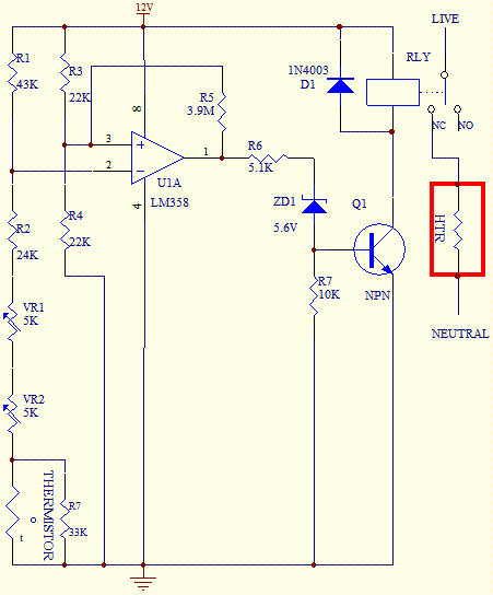
HVAC thermostat has been one of the common device used in residential and industrial buildings to control the temperature of a space be it a warehouse, a room, a hall or an office. This thermostat project will focus on the heating control of a space that uses electric heater as its source of heating. It basically consists of a comparator that controls the ON and OFF of the electric heater based on the sensor temperature.
The control of the fan speed is usually hardwired with two speed or three speed motors and is incorporated into the thermostat. The temperature range of this thermostat is from 5 Celcius to 30 Celcius with a tolerance of approximately 3 degree Celcius. Hence, only non critical tolerance control of temperature control such as a room can be used.
Circuit Description
The circuit diagram shows the configuration of the HVAC thermostat. The LM358 Op Amp is used as a comparator to sense the inputs of the reference voltage (PIN 3) and room temperature (PIN 2). The thermistor used is a NTC (negative temperature coefficient) type where its resistance will drop when the temperature increases and vice versa. It has a resistance of 20K ohm at 25 degree Celcius. When the room temperature drops, the thermistor resistance will go up and hence the output of the operational amplifier will be low. This cause the relay to turn OFF and the heater will conduct until the temperature of the room rises again.

The circuit is calibrated using variable resistor VR1. Set the lever of the slide potentiometer or rotary potentiometer VR2 to 25 Celcius location. Place the thermistor at a space where the temperature is at 25 Celcius. By varying VR1, set the resistance at the position between the ON and OFF of the relay. Use a suitable contact relay rating according to the load of the heater.
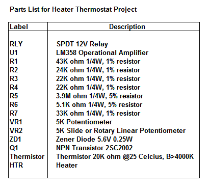
Parts List
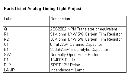
Analog Timing Light Project
Timing Light Project
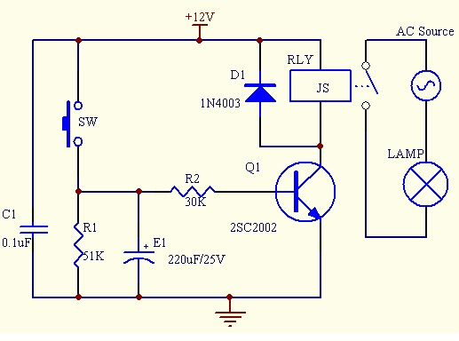
This analog timing light project uses RC circuit as a delay OFF timer to control the duration an incandescent light turns ON. When the accuracy of a timer is not critical, the use of RC circuit is a good choice as it is more cost effective and simple. Once the normally open switch SW is pressed, the light will turn ON for a duration of 10 - 20 seconds before it turns OFF. The duration of the turn ON time can be varied by varying the values of R1, R2 and E1.
Schematic Diagram
The schematic of the project is as shown below.
When SW is pressed, the base of the transistor Q1 is forward bias and it turns ON. This turns ON the 12V relay that is connected to the transistor. The contact of the relay RLY must be able to withstand the current of the load. At the same time, the electrolytic capacitor E1 is being charged to a voltage of approximately 0.7V.
Once SW is released, E1 will discharged through resistor R2 and the base of the transistor. After some time, When the voltage across E1 drops to approximately 0.5V, the transistor will turn OFF. This in turn will cause the relay to turn OFF and the incandescent light will turn OFF. The timing of the turn OFF can be changed by changing the values of E1, R1 and R2.
Parts List
The parts list of the project is as shown below.
Bar Graph LED Project
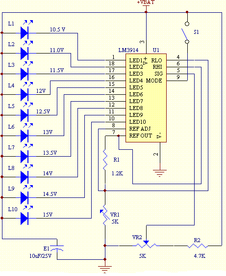
This bar graph LED battery level indicator project is based on LM3914 monolithic IC from National Semiconductor that senses the voltage levels of the battery and drives the 10 light emitting diodes based on the voltage level that is detected. It provides a linear analog display output and has a pin that can be configured to display the output in moving dot or bar graph. The current driving the LEDs is regulated and programmable hence limiting resistors are not required.
The schematic shows how the various components are connected. Switch S1 is used to change the display type from moving dot to bar graph type. When S1 is ON, the display type is bargraph but when it is OFF the display changes to moving dot type. VR1 is used to set the lower limit of the display. By using a variable DC power supply, set the VBAT to 10.5V. Adjust VR1 until the LED L1 turns ON. Next, set the VBAT to 15V, adjust VR2 until all the LEDs turn ON (When S1 is ON). The specifications of LM3914 can be obtained from National Semiconductor Website.
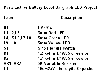
Parts List
Smart Cameras in Embedded Systems
A smart camera performs real-time analysis to recognize scenic elements. Smart cameras are useful in a variety of scenarios: surveillance, medicine, etc.We have built a real-time system for recognizing gestures. Our smart camera uses novel algorithms to recognize gestures based on low-level analysis of body parts as well as hidden Markov models for the moves that comprise the gestures. These algorithms run on a Trimedia processor. Our system can recognize gestures at the rate of 20 frames/second. The camera can also fuse the results of multiple cameras
Overview
Recent technological advances are enabling a new generation of smart cameras that represent a quantum leap in sophistication. While today's digital cameras capture images, smart cameras capture high-level descriptions of the scene and analyze what they see. These devices could support a wide variety of applications including human and animal detection, surveillance, motion analysis, and facial identification.
Video processing has an insatiable demand for real-time performance. Fortunately, Moore's law provides an increasing pool of available computing power to apply to real-time analysis. Smart cameras leverage very large-scale integration (VLSI) to provide such analysis in a low-cost, low-power system with substantial memory. Moving well beyond pixel processing and compression, these systems run a wide range of algorithms to extract meaning from streaming video.
Because they push the design space in so many dimensions, smart cameras are a leading-edge application for embedded system research.
Detection and Recognition Algorithms
Although there are many approaches to real-time video analysis, we chose to focus initially on human gesture recognition-identifying whether a subject is walking, standing, waving his arms, and so on. Because much work remains to be done on this problem, we sought to design an embedded system that can incorporate future algorithms as well as use those we created exclusively for this application. Our algorithms use both low-level and high-level processing. The low-level component identifies different body parts and categorizes their movement in simple terms. The high-level component, which is application-dependent, uses this information to recognize each body part's action and the person's overall activity based on scenario parameters. Low-level processing The system captures images from the video input, which can be either uncompressed or compressed (MPEG and motion JPEG), and applies four different algorithms to detect and identify human body parts.
Region extraction: The first algorithm transforms the pixels of an image into an M ¥ N bitmap and eliminates the background. It then detects the body part's skin area using a YUV color model with chrominance values down sampled Nextthe algorithm hierarchically segments the frame into skin-tone and non-skin-tone regions by extracting foreground regions adjacent to detected skin areas and combining these segments in a meaningful way.
Contour following: The next step in the process involves linking the separate groups of pixels into contours that geometrically define the regions. This algorithm uses a 3 ¥ 3 filter to follow the edge of the component in any of eight different directions.
Ellipse fitting: To correct for deformations in image processing caused by clothing, objects in the frame, or some body parts blocking others, an algorithm fits ellipses to the pixel regions to provide simplified part attributes. The algorithm uses these parametric surface approximations to compute geometric descriptors for segments such as area, compactness (circularity), weak perspective invariants, and spatial relationships.
Graph matching: Each extracted region modeled with ellipses corresponds to a node in a graphical representation of the human body. A piecewise quadratic Bayesian classifier uses the ellipses parameters to compute feature vectors consisting of binary and unary attributes. It then matches these attributes to feature vectors of body parts or meaningful combinations of parts that are computed offline. To expedite the branching process, the algorithm begins with the face, which is generally easiest to detect.
Thursday, 1 July 2010
Simple Home Security Monitoring Project
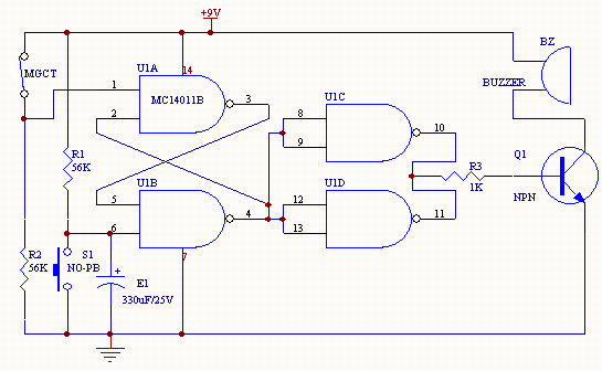
This project is a standalone simple home security monitoring project that will trigger a buzzer when the magnetic contact is opened. Magnetic contacts are usually NC (Normally Closed) and are used on doors and windows. They consists of two parts namely a magnet and a reed switch. When the reed switch is in close proximity to the magnet, the switch will close and vice versa. Usually the magnet is fitted to the door and the reed switch is fitted to the door frame in close proximity to one another such that when the door is closed, the two parts are in close contact and hence the switch is closed. When the door is opened, the magnet will be a distance away from the reed switch and hence the switch will open.
Circuit Description
The circuit shown below is a basic latching circuit consisting of a quad 2-input NAND Gate IC. It is configured such that the flip flop circuit U1A and U1B has both its input held at logic "1". Pin 1 is held at logic "1" by the magnetic contact and pin 6 is held at logic "1" by resistor R1. S1 switch is a normally open pushbutton switch which is used as a reset button. When S1 is pressed, the input pin 6 will be at logic "0", hence the output of U1B will go to logic "1". This logic is inverted by U1C and U1D to logic "0". The transistor Q1 will be OFF and buzzer will not sound.

When the magnetic contact sensor is opened, the input to pin 1 will be at logic "0", giving an output of logic "1" at pin 3 of U1A. Pin 5 of U1B will go "1" and pin 6 will be "1" as well giving an output at pin 4 a logic "0". This will be inverted and a logic "1" will be generated at the base of transistor Q1. The transistor Q1 will turn ON and cause the buzzer to sound continuously until the reset switch S1 is pressed.
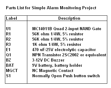
Parts List
The parts list of the project is given below.

Friday, 4 June 2010
Automatic car parking indicator using Microcontroller
Description:
Conventionally, car parking systems does not have any intelligent monitoring system. Parking lots are monitored by human beings. All vehicles enter into the parking and waste time for searching for parking slot. Sometimes it creates blockage. Condition become worse when there are multiple parking lanes and each lane have multiple parking slots.
Use of automated system for car parking monitoring will reduce the human efforts. Display unit is installed on entrance of parking lot which will show LEDs for all Parking slot and for all parking lanes. Empty slot will be indicated by glowing the respective LED.
Block Diagram: |
Description: |
Pick and Place robot
INTRODUCTION:
In this highly developing society; time and man power are critical constrains for completion of task in large scales. the automation is playing important role to save human efforts in most of the regular and frequently carried works e.g. most of the industrial jobs like welding, painting, assembly, container filling etc. one of the major and most commonly performed work is picking and placing of jobs from source to destination. For this purpose, ‘pick and place robot ‘maybe used.
The pick and place robot is a microcontroller based mechatronic system that detects the object, picks that object from source location and places at desired location. For detection of object, infrared sensors are used which detect presence of object as the transmitter to receiver path for infrared sensor is interrupted by placed object. As soon as robot senses presence of object, it moves towards object, picks it with end effectors, and moves along way gantry and finally place it on destination.
If another object causes interrupt, it again does the same job. Whole process is controlled by micro controller.
Block Diagram: |
DESIGN SPECIFICATIONS:
ADC Interface ---- 4 channel (expandable) to detect object position.
Supply Voltage ---- 230V (AC).
8 bit microcontroller – P89V51RD2.
Motor interface – 3 motors : 2 motors in parallel.
MECHANICAL DESIGN:
This pick and place robot has two main mechanical components:
A] Robotic arm and end-effectors.
B] Gantry for moving the arm.
OPERATION OF ROBOT :
1. Initially we will assume the rest position of entire system, i.e. state when no object is placed.
2. At this stage, photo detector is having its output high, since receiver of sensor can receive photons from transmitter as no object I in its path to interrupt.
3. As soon as object is placed at the picking platform, the sensor gets interrupted and outputs low. This signal is sent to the microcontroller which is burnt with program which tells what operation is to be performed at this stage.
4. For understanding operation, let us rename the two motors used here. Let the name of gantry motor be M1 and that for end effecter motor is M2.
5. Now as microcontroller detects that object is placed, it moves motor M1 in say clockwise direction for a fixed time due to which whole arm moves towards picking platform.
6. As it reaches there, M1 stops and now motor M2 is started in say clockwise direction to hold the object by closing jaw. This motor also, is on for particular fixed time instant.
7. As M2 gets off, motor M1 is moved again in opposite (here anticlockwise) direction till the time it reaches the placing platform.
8. As it reaches placing platform, the motor M1 stops and M2 is switched ON in opposite (here anticlockwise) direction till it releases object properly on desired place.
9. If after this no object is detected, the robot is in rest position. Otherwise if another object is detected, steps from 3 are repeated till step 8.
BLOCK DIAGRAM DESCRIPTION:
I] ADC:
1. We are using an 8 bit ADC PCF 8591, which uses an I2C bus protocol. It has 4 analog input channels AIN1, AIN2, AIN3 & 1 analog output channel AOUT. > Pin no. 1 i.e. channel 1 is connected IR sensor.
2. Except for the micro controller AT 89V51RD2, there is no other peripheral device connected to the ADC. Hence the hardware address lines (A0, Al & A2) are grounded.
3. Pin no. 9 and 10 are serial data line (SDA) and serial clock line (SCL) respectively. Both lines must be connected to a positive supply through a pull-up resistor. These pins are connected to the P1.6 & P1.7 of the micro controller.
4. Here we are not feeding the OSC (pin no. 11) with an external clock Signal, but using the ON chip oscillator. Hence the EXT pin (pin no.12) is directly grounded.
5. Vref (pin no. 14) is connected to the 5 V regulated supply.
II] Microcontroller: 1. PORT 0: (PIN NO. 39- PIN NO. 32): P0.0— P0.7 of the micro controller is connected to the motor driver circuit.
2. Pin no. 9 is RESET pin, which is connected to the reset circuit.
3. Pin no. 9 and 10 of ADC are serial data line (SDA) and serial clock line (SCL) respectively. Both are connected to a positive supply through a pull-up resistor. These pins are connected to the P1.6 & P1.7 of the micro controller.
III] DRIVER CIRCUIT:
1. The L293 and L293D are quadruple high-current drivers.TheL293is designed to provide bidirectional drive currents of up to 1 A at voltages from 4.5 V to 36 V. The L293D is designed to provide bidirectional drive currents of up to 600-mA at voltages from 4.5 V to 36 V. Both devices are designed to drive inductive loads such as relays, solenoids, dc and bipolar stepping motors, as well as other high-current/high-voltage loads in positive-supply applications.
2. All inputs are TTL compatible. Each output is a complete totem-pole drive circuit, with a Darlington transistor sink and a pseudo-Darlington source. Drivers are enabled in pairs, with drivers 1 and 2 enabled by 1,2EN and drivers 3 and 4 enabled by 3,4EN.
3. When an enable input is high, the associated drivers are enabled and their outputs are active and in phase with their inputs. When the enable input is low, those drivers are disabled and their outputs are off and in the high-impedance state. With the proper data inputs, each pair of drivers forms a full-H (or bridge) reversible drive suitable for solenoid or motor applications.
4. A Vcc1 terminal, separate from Vcc2, is provided for the logic inputs to minimize device power dissipation.
APPLICATIONS:
1. It can be used in Production industry.
2. In mass production.
3. In Automobile Industry.
FUTURE SCOPE:
1. Bottle filling Plant.
2. Construction works.
REFERENCES:
1. Programming Microcontroller 8051 and customizing By Myke Predko
2. 8051 Microcontroller By Mazidi and Mazidi
3. 8051 Microcontroller By Kenneth Ayala
| Sr no. | Component | Quantity | Cost(Rs) |
| 1 | Transformer 12V, 1A | 1 | 55 |
| 2 | Diode 1N4007 | 4 | 5 |
| 3 | Electrolytic capacitor 2200uf, 25V | 1 | 3 |
| 4 | Capacitor 100uf | 2 | 5 |
| 5 | IC 7805 | 1 | 8 |
| 6 | IC 7812 | 1 | 8 |
| 7 | Crystal 11.0592Mhz | 1 | 20 |
| 8 | IC L293d | 1 | 95 |
| 9 | P89V51RD2 | 1 | 125 |
| 10 | PCF8591 | 1 | 125 |
| 11 | IC Socket 40pin DIP | 1 | 20 |
| 12 | IC Socket 16pin DIP | 2 | 10 |
| 13 | 2 pin connector | 4 | 20 |
| 14 | PCB 4*4 | 1 | 20 |
| 15 | PCB 6*4 | 1 | 25 |
| 16 | PCB | 1 | 25 |
| 17 | Resistors | 5 | 3 |
| 18 | Miscellaneous | 10 | |
| 19 | Mechanical assembly | 900 |