
-
Mobile phone (DTMF) controlled electrical device switching
-
Automatic advanced Railway gate Control System.
-
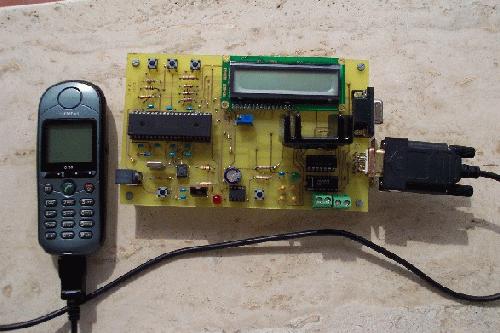
Digital Realtime Clock Implementation with Microcontroller and LCD.
-
Industrial conveyer belt object counting system.
-
Intelligent High Power LED Street light Control System.
-
Digital Frequency Meter with LCD Display
-
IR Remote Controlled Realtime Clock with LCD display
-
Transformer realtime temperature monitoring and thermal Overload protection
-
Digital RPM Indicator for Electrical Motor with Over speed alarm Indicator
-
Infrared Remote based Electrical Device Control with Triac and Optically Isolated Diac
-
Infrared Remote controlled High Voltage device switching with Electromagnetic Relay
-
IR TV remote controlled DC Motor speed controller with password protection
-
IR TV remote controlled Stepper Motor controller with password protection
-
LDR based automatic lamp illumination controller with High Power/Intensity LED lighting (PWM control)
-
Optically Isolated Fuse blown Indicator with Sound and light indicator
-
High Voltage Fuse blown Indicator with Display on Computer/PC
-
Pulse Width Modulation (PWM) Speed Control of a DC Motor
-
IR LED and LDR based Heartbeat Monitor with display on LCD.
-
IR LED and LDR baaed Heartbeat Monitor with display on Computer/PC.
-
Temperature Controlled Fan (DC Motor based with PWM).
-
Realtime Car battery monitoring and low voltage alert system.
-
Automatic room light intensity based window blinds control system.
-
Temperature based ceiling fan speed control system (230v AC Motor).
-
Automatic Irrigation water supply monitoring and control system.
-
Infrared remote controlled garage door control system.
-
Automatic washing machine motor control system.
-
Vehicle inside and outside temperature monitoring system.
-
Wireless split AC blower and compressor control system.
-
Industrial and Home Security System based projects using various sensors like smoke, Fire, GAS, Temperature, PIR, IR, RF etc.
-
Digital RPM indicator on LCD display (Used in latest Bikes and Cars etc.)
-
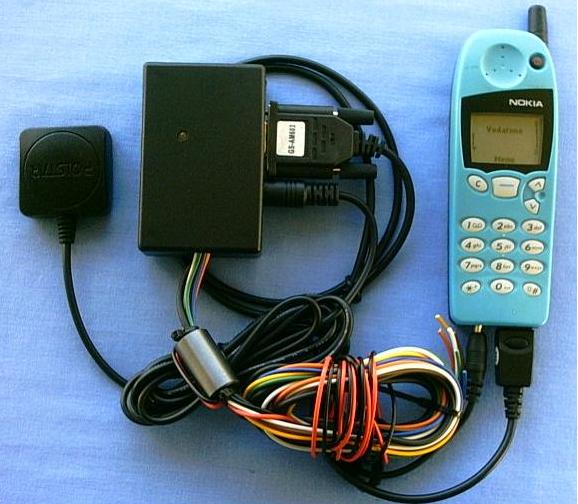
GPS speedo meter with Over speed alert system.
-
GPS and microcontroller based location (latitude and longitude) display On lcd display
-
Microcontroller based GPS Clock. It maintains accurate time based on the signals received from the satellites.
-
GPS and Microcontroller based Geographical location Identification System.
-
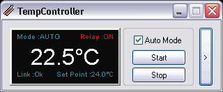
Digital Thermostat with LCD Temperature Display.
-
Embedded Realtime Clock based Industrial Devices Control System.
-
GPS Based Train/Bus Station Indication System with display on LCD.
-
GPS based Speedo meter (Used in Boats,Ships, Aero planes etc).
-
Microcontroller based digital Over voltage Protection system for industrial loads.
-
Radio Frequency (RF 433 MHz) based Industrial Wireless Device Control System.
-
Microcontroller based advanced automatic city street control system.
-
Industrial Advanced Temperature monitoring and Control System.
-
Microcontrolle based water level monitoring and control system.
-
Microcontroller based Digital Alpha-numeric message scrolling Display.
-
Automatic intrusion Alarm/Alert System.
-
Digital Energy Meter LCD display.
-
Radio Frequency based Realtime Child monitoring and alarm system.
-
Realtime burglar alarm system using PIR Sensor (Passive Infrared Sensor)
Popular Posts
-
Introduction This amplifier does not claim to be "state of the art", and in fact the base design is now over 20 years old. It is ...
-
RESEQUENCING ANALYSIS OF STOP-AND-WAIT ARQ FOR PARALLEL MULTICHANNEL COMMUNICATIONS:--DOTNET--2009 RESEQUENCING ANALYSIS OF STOP-AND-WAIT AR...
-
Signals, including those used for communication between occupants of a car or train.Indicators, recorders, telegraphic, telephonic, or oth...
Saturday, 18 September 2010
List of Microcontroller based Mini Projects
Mechanical Engineering Projects
-
SPM for grinding of Radome Shell (Internal grinding to reduce the weight)
-
Design of cam for radial shell grinding (CAM profile for copying attachment)
-
Fixture design for VMC (Cylinder Head)
-
Fixture design for HMC (Cylinder Head)
-
Process Capable Tolerancing (Setting proper tolerances early in the design phase to achieve quality production and reducing production cost)
-
Reverse Engineering process (3D scanning developing 3D surface or point data, converting 3D point data to virtual design and manufacturing the model with desired alterations)
-
Composite material analysis in cosmos
-
Check valve flow analysis Cosmo Floworks
-
Manufacturing Process & process planning for a component or Job
-
Process tooling for complete production cycle (Tool Design)
-
Combination Tool Design
Robotics Projects
-
Radio Frequency based remote controlled robot with wireless video camera mounted on it.
-
Autonomous Robot with artificial vision for obstacle detection.
-
Accelerometer (Gyroscope) Controlled Robot. Accelerometer is mems based 3-axis sensor that can sense the tilt in of the 3-diamentions. The robot moment is controlled based on the tilt angle of the robot. No need to press any buttons for robot control.
-
Touch Screen Controlled intellegent robot.
-
Live Human being detection wireless remote controlled Robot. (Useful for detection of terrorists hiding inside buildings).
-
GSM (SMS) Mobile Phone Controlled Intelligent Robot.
-
Micro Electro Mechanical Sensor (MEMS) Accelerometer/Gyroscope based self-balancing robot.
-
Mobile phone controlled four-legged walking robot with speed and direction control.
-
Radio Frequency (RF) Controlled Wireless Robot.
-
Infrared Light tracing Robot (TV Remote controlled).
-
Visible light follower Robot.
-
Accelerometer (Gyroscope) Controlled Robot.
-
DTMF based Mobile phone controlled Robot.
-
Obstacle detection robot with mechanical sensing switches.
-
Line Follower Robot.
-
Live Human detection and alerting Robot.
-
Remote Controlled Land Rover.
-
PC Controlled Wired Robot.
-
PC Controlled Wireless Robot.
-
Obstacle detection Robot with Ultrasonic Sensors.
-
Wall Follower Robot.
-
Robot Controlled Wireless Audio-Video Streaming Camera.
DTMF Controlled Wireless Robot
The mobile unit which is dedicated at the robot is interfaced with an intellectual device called Microcontroller so that it takes the responsibility of decoding the tones received and perform the corresponding predefined tasks such as move front or back, left or right etc.
The micro controller is also interfaced with few DC motors in order to move the robot in different directions. The ON and OFF of the DC motors depends on the direction it has to move which is the complete responsibility of the controller to take those intelligent decisions.
The major building blocks of this project are:-
- Regulated Power Supply
- GSM Modem/Phone
- Microcontroller based Control Unit
- Robot Mechanical Assembly
- DTMF Drivers
Wireless Accelerometer Controlled Robot
The aim of this project is to build a vehicle that can be controlled by using wireless MEMS (Micro Electro-Mechanical Systems) based accelerometer. This consists of a remote control that wirelessly transmits data using RF technology to the remote vehicle to move in any direction. The accelerometer will be mounted on a steering plate (remote control), such that if the steering plate leans in some direction then the robot vehicle moves in that direction.
If the user wants to move the robot forward he can lean the steering plate forward and backward for reverse. To turn left or right user need to turn the steering plate toward left or right respectively.
The major building blocks of this project are:
- Two Microcontroller Mother Boards with regulated power supply.
- 433MHz RF Transmitter and Receiver Modules.
- Accelerometer Sensor Module.
- Robot Vehicle with two PWM controlled DC Motors.
GSM (SMS) Controlled Wireless Robot
“GSM (SMS) Controlled Wireless Robot” is automatic robots which capable of receiving a set of command instructions in the form of Short message service and performs the necessary actions. We will be using a dedicated modem/mobile at the receiver module i.e. with the robot it self and send the commands using SMS service as per the required actions.
The mobile unit which is dedicated at the robot is interfaced with an intellectual device called Micro controller so that it takes the responsibility of reading the received commands in the form of SMS from the mobile unit and perform the corresponding predefined tasks such as move front or back, left or right etc. The micro controller is also interfaced with few DC motors in order to move the robot in different directions. The ON and OFF of the DC motors depends on the direction it has to move which is the complete responsibility of the controller to take those intelligent decisions.
The major building blocks of this project are:-
- Regulated Power Supply
- GSM Modem
- Microcontroller based Control Unit
- Robot
- Serial Communication Port(RS232)
Friday, 17 September 2010
Hadoop seminar
Computing in its purest form, has changed hands multiple times. First, from near the beginning mainframes were predicted to be the future of computing. Indeed mainframes and large scale machines were built and used, and in some circumstances are used similarly today. The trend, however, turned from bigger and more expensive, to smaller and more affordable commodity PCs and servers.
Most of our data is stored on local networks with servers that may be clustered and sharing storage. This approach has had time to be developed into stable architecture, and provide decent redundancy when deployed right. A newer emerging technology, cloud computing, has shown up demanding attention and quickly is changing the direction of the technology landscape. Whether it is Google’s unique and scalable Google File System, or Amazon’s robust Amazon S3 cloud storage model, it is clear that cloud computing has arrived with much to be gleaned from.
Cloud computing is a style of computing in which dynamically scalable and often virtualizes resources are provided as a service over the Internet. Users need not have knowledge of, expertise in, or control over the technology infrastructure in the “cloud” that supports them.
Need for large data processing
We live in the data age. It’s not easy to measure the total volume of data stored electronically, but an IDC estimate put the size of the “digital universe” at 0.18 zettabytes in 2006, and is forecasting a tenfold growth by 2011 to 1.8 zettabytes.
Some of the large data processing needed areas include:-
• The New York Stock Exchange generates about one terabyte of new trade data per day.
• Facebook hosts approximately 10 billion photos, taking up one petabyte of storage.
• Ancestry.com, the genealogy site, stores around 2.5 petabytes of data.
• The Internet Archive stores around 2 petabytes of data, and is growing at a rate of 20 terabytes per month.
• The Large Hadron Collider near Geneva, Switzerland, will produce about 15 petabytes of data per year.
The problem is that while the storage capacities of hard drives have increased massively over the years, access speeds—the rate at which data can be read from drives have not kept up. One typical drive from 1990 could store 1370 MB of data and had a transfer speed of 4.4 MB/s,§ so we could read all the data from a full drive in around five minutes. Almost 20 years later one terabyte drives are the norm, but the transfer speed is around 100 MB/s, so it takes more than two and a half hours to read all the data off the disk. This is a long time to read all data on a single drive—and writing is even slower. The obvious way to reduce the time is to read from multiple disks at once. Imagine if we had 100 drives, each holding one hundredth of the data. Working in parallel, we could read the data in under two minutes.This shows the significance of distributed computing.
Electrical Engineering Projects
-
Mobile technology (GSM) based remote monitoring and control of digital Energy meter. Useful for Electricity Department personal for remote meter reading. Also useful to disconnect the power supply to consumer incase of non-payment of electric bill. This is also used to exchange messages like power cut timings with the consumers.
-
DC Motors speed synchronization for rolling mills.
-
Touch Screen based digital devices control system. This project is to build a Graphical LCD Touch Screen interface for switching electrical devices. The controlled devices can be of high voltage or low voltage.
-
Wireless Energy Meter monitoring system with automatic tariff calculation.
-
DC Motor Speed and direction control over GSM Mobile/Modem.
-
Energy meter per-day average, Max and Min Load display on Graphical LCD.
-
MMC/SD card based data logger for energy meter with time and KWH readings for historical data logging and analysis.
-
PIR based energy conservation system for corporate Computers and lighting system.
-
Wireless power theft monitoring system and indication at local substations.
-
Touchscreen controlled lamp dimmer for next generation apartments.
-
Microconroller and Touchscreen controlled motor speed and direction controlling system.
-
Touchscreen operated industrial oil dispensing system (OIL SCADA).
-
Dual (active and standby) Lithium-ion battery charger for continuous non-interrupted power supply to critical loads.
-
Graphical LCD and Touch Screen based Electrical devices control system.
-
Implementation of wireless sensors network based industrial temperature monitoring system.
-
Touchscreen based advanced temperature monitoring and control system with graphical LCD.
-
GSM based Irrigation Water Pump Controller for Illiterates. (No Mobile phone operation knowledge required).
-
Triac and optically isolated diac based electrical oven temperature monitoring and controlling system with zero-crossing detector.
-
High power LED based intelligent streetlight controlling system with automatic brightness control with vehicle presence sensor.
-
Timer based Electrical Oven temperature monitoring and control for Metal Industries.
-
GSM based SCADA implementation using Microcontroller.
-
Microcontroller based Substation Monitoring and control.
-
Microcontroller based Generator/Alternator Control and Monitoring System
-
Electrical Data (voltage, current, frequency etc...) Logger. The purpose of this project is to log electrical data at remote locations like substations. The data is sensed using various electrical sensors and processed by microcontroller. This processed data is stored in a MMC memory stick connected to the microcontroller board. This data can be downloaded to computer for further processing.
-
Microcontroller based Single phasing preventor.
-
Microcontroller based Solar Tracker with Stepper Motor Control.
-
PWM based DC Motor Closed loop Speed Controller.
-
Frequency Locked Loop (FLL) DC Motor Speed Control
-
Radio Frequency (RF) based Wireless Control Of DC/Stepper Motor Speed Control.
-
RF based Wireless Electrical Devices Controller.
-
Motor Speed Monitoring over GSM Mobile.
-
Microcontroller based refrigeration control system.
-
Timer based automatic power cutoff for industrial sealing/packaging machines.
-
Wireless SCADA.
-
GSM/Mobile/Cell Phone Based Device Monitoring and Control.
-
GSM Based Automatic Irrigation Water Controller System
-
Automatic Intelligent Plant Watering System
-
IR (Infrared) Remote based Stepper Motor Speed and Direction Controller
-
RC5 IR Based Remote Device Switching
-
The Robot that follows the (Infrared) Light
-
Frequency Locked Loop DC Motor speed monitoring and control system.
-
Digital Tachometer (Non-contact)
-
Digital Voltage, Current and Frequency Meter.
-
SCADA system design and construction for real-time electrical parameter monitoring and control.
-
Transformer oil temperature monitoring with automatic Circuit Breaker operation.
-
GSM/Mobile/Cell Phone Based Device Monitoring and Control System.
-
Substation Fuse blown Indicator.
-
Mobile phone controlled Street Light monitoring and control system.
-
UPS battery monitoring system over GSM for high availability systems (banking/finance/medical etc).
-
DTMF mobile phone controlled dam water gates controlling system with high-level protection.
-
DC Motor Speed and direction control using RF/IR/Zigbee technologies.
-
Hazardous chemical valve control system with stepper motor and line of site remote control.
-
Contact less Motor speed monitoring on Graphical display with high and low speed alerts.
-
Design and construction of Earth fault relay for single phase power system.
-
RF transceiver (Zigbee/X-Bee) based energy meter monitoring system. (Energy Meter reading on PC over wireless comm.)
-
Talking energy (KWH) meter.
-
Password enabled pre-paid liquid/milk dispensing system.
- High voltage fuse blown indicator with display on PC with optical isolation between PC and HV bus bars.
Touch Screen GLCD based Digital Devices Control System
The aim of this project is to build a Graphical LCD Touch Screen interface for switching electrical devices. The controlled devices can be of high voltage or low voltage. A virtual on screen keypad and control board can be developed by the program running inside microcontroller. The status of devices can be viewed on Graphical LCD. No needs to have mechanical push buttons or LED indicators. Users can control the devices with gentle finger touch. Controlling of Electrical appliances such as Television can be Passwordprotected. By this we can limit the access to certain electrical devices to children or any other un-authorized persons. | ||
Electronics Engineering Projects
- Construction of microcontroller based Touchscreen Mobile Phone with Password protected features.
- Touch Screen GLCD based Digital Devices Control System
- MEMS Accelerometer based tilt operated Graphical LCD and memory stick based textbook reading system.
- GSM Based Automatic Energy Meter Reading System
- Microcontroller based GPS Data Logger into MMC/SD Card.
- Triac and optically isolated diac based electrical oven temperature monitoring and controlling system with zero-crossing detector.
- GSM based Irrigation Water Pump Controller for Illiterates. (No Mobile phone operation knowledge required)
- Implementation of location based advertisement system using GPS and Graphical LCD.
- Innovative keyboard construction with only one input pin.
- RFID and GSM based intelligent letterbox (mailbox).
- Wireless energy meter monitoring system with automatic tariff calculation on handheld.
- Image based password authentication for Illiterates with Touchscreen.
- Speaking microcontroller for deaf and dumb.
- Wireless GoogleEarth control system at Railway/Bus Stations for tourist’s route map guidance.
- Virtual wireless dancing bells for classical dancers.
- Touchscreen based temperature monitoring and control system with graphical LCD.
- Location driven car music player. (Plays devotional songs near temples, shuts at home etc.)
- GPS based asset/vehicle/animal/child tracking system.
- Microcontroller and Touchscreen based wireless library book catalog system.
- Touchscreen based Nurse/attendant calling system for physically impaired.
- Graphical LCD and Memory stick (MMC/SD card) based textbook reading system.
- Mobile phone controlled four-legged walking robot with speed and direction control.
- GPS based universal clock. Gets the time from satellites and displays on GLCD.
- Microcontroller based online examination system with dynamic questions.
- Digital vehicle speedometer with password enabled speed limit setting.
- GPS based vehicle travel location-logging system. This System stores the traveler’s geographical location and speed at an interval of one second and is stored in to 1GB MMC/SD memory card.
- SMS based remote SIM card’s address book access system.
- Microcontroller based digital clock with Graphical LCD and Sanskrit font (or Any regional font) Numbers.
- Microcontroller based virtual boundary/fencing for Wild Animals.
- GSM based instantaneous vehicle registration details extraction system very useful for Traffic police.
- Wireless Heartbeat Monitoring and Alert system.
- RFID/Mifare/Smart Card based security access control systems.
- GPS and GSM based real-time vehicle tracking on GoogleEarth (with two GSM Modems)
- Implementation of wireless sensors network for Wild Fire monitoring system.
- Real-time Heartbeat Monitoring system with display on Graphical LCD and Voice based alerting system.
- Touchscreen operated liquid dispensing system.
- Infrared (IR) remote controlled Muscle Stimulator with duration and intensity control.
- GPS based border alert system for fishermen.
- MEMS Accelerometer based digital photo frame with automatic position/view adjustment system (similar to digital cameras).
- Construction of Touchscreen based portable Digital Clock.
- GPS and Graphical display based tourist-guiding system with Touchscreen keyboard input for dynamic location recording. This can be used any where in the world including Sea and Forest locations.
- Microcontroller and RF transceiver based chatting application with Touchscreen keyboard implementation.
- Travel assistant for blind with dynamic user input for location based alerts.
- Telugu Tutor with dynamic text and Images identification for elementary school kids.
- Micro Electro Mechanical Sensor (MEMS) Accelerometer/Gyroscope based self-balancing robot.
- Military persons training system that monitors the speed at which they move and records the calculated traveled distance with the time.
- GPS based office cab monitoring system very useful for the safety of female employees. This system records the travel path and location with timings. Also records the destination of each employee home.
- GPS based station name announcement and display system for Trains/buses.
- Microcontroller and voice based alerting system for blind people with GPS enabled location identification.
- GPS based navigator with location display on Graphical LCD. This provides user to have the location information displayed in any language.
- Advanced GPS based navigator for illiterates.
- Live Human being detection wireless remote controlled Robot. (Useful for detection of terrorists hiding inside buildings)
- Radio Frequency based remote controlled robot with wireless video camera mounted on it.
- Autonomous Robot with artificial vision for obstacle detection.
- Accelerometer (Gyroscope) Controlled Robot. Accelerometer is mems based 3-axis sensor that can sense the tilt in of the 3-diamentions. The robot moment is controlled based on the tilt angle of the robot. No need to press any buttons for robot control.
- Mobile technology (GSM) based remote monitoring and control of digital Energy meter. Useful for Electricity Department personal for remote meter reading. Also useful to disconnect the power supply to consumer incase of non-payment of electric bill. This is also used to exchange messages like power cut timings with the consumers.
- Microcontroller and GPS based geographical map drawing instrument. Very useful for Civil engineers.
- Touchscreen controlled motor speed and direction controlling system.
- GSM based digital Notice board with display on Monitor or LCD display.
- PIR based energy conservation system for corporate Computers and lighting system.
- Remote control of critical software applications with mobile phone.
- Microcontroller based dual Lithium-ion battery charger with automated charge and discharge cycles.
- Virtual distance measuring tape with Graphical LCD. Very useful for roads and buildings department. One man operable and works on anywhere on earth.
- Radio Frequency wireless remote controlled digital camera with high power LED based focusing light. The camera direction can be controlled remotely and the video images can be seen live on TV.
- Wireless Speedo meter for boat/ship with speed and location limit alerts.
- GPS based travel assistant for blind people.
- Touch Screen based digital devices control system. This project is to build a Graphical LCD Touch Screen interface for switching electrical devices. The controlled devices can be of high voltage or low voltage.
- GSM Mobile phone controlled intelligent Robot.
- Automatic Intelligent Plant Watering System.
- DC Motor Speed and direction control over GSM Mobile/Modem.
- Mobile phone controlled Street Light monitoring and control system.
- UPS battery monitoring system over GSM for high availability systems (banking/finance/medical etc).
- Touchscreen controlled lamp dimmer for next generation apartments.
- Soil Moisture sensor based intelligent irrigation water pump controlling system with GSM technology.
- DTMF mobile phone controlled dam water gates controlling system with high-level protection.
- DC Motor Speed and direction control using RF/IR/Zigbee technologies.
- Hazardous chemical valve control system with stepper motor and line of site remote control.
- Contact less Motor speed monitoring on Graphical display with high and low speed alerts.
- Liquid dispensing system with adjustable quantity for industrial use.
- Password enabled pre-paid liquid/milk dispensing system.
- Wireless Energy Meter monitoring system with automatic tariff calculation.
- Data logger for energy meter with time and KWH readings. Very useful for historical data logging and analysis.
- High voltage fuse blown indicator with Voice based announcement system.
- Voice enabled devices switching for visually impaired.
- RF transceiver (Zigbee/X-Bee) based energy meter monitoring system. (Energy Meter reading on PC over wireless comm.)
- GSM based SCADA (Supervisory Control and Data Acquisition) implementation.
- SCADA system design and construction for real-time electrical parameter monitoring and control.
- Timer based Electrical Oven temperature monitoring and control for Metal Industries.
- Timer based automatic power cutoff for industrial sealing/packaging machines.
- GPS & GSM Based Car Security System.
Easy to find the stolen Car. Global Positioning Sytem (GPS) has been used in various commercial applications including transportation, navigation and vehicle position tracking, which when coupled with GSM mobile phone technology, the technology can help locate stolen vehicle and retrieval process.
 (GPS+GSM+Microcontroller)
- Standalone GPS Coordinates(Latitude,Longitude...) Locater. (GPS+Microcontroller+LCD)
The purpose this project is to get the Latitude and Longitude from the satellites and display them on LCD display.
- GPS & GSM Based Realtime Vehicle Tracking System.
This system locates the Vehicle on the earth by the use of GPS and sends the co-ordinates (Longitude & Latitude), Time and Vehicle speed to the owner of the vehicle using GSM Modem.
(GPS+GSM+Microcontroller)
- Microcontroller driven GPS Clock (GPS+Microcontroller+LCD)
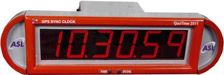
This updates time (GMT) from satellites and displays on LCD.
- GSM/Mobile/Cell Phone Based Device Monitoring and Control Ststem.
The purpose of this project is to Monitor and Control any Digital or Analog devices from your Cell Phone. This Project can be used to control up to 16 electrical devices. With this circuit you can switch-ON , OFF or Restart some Linux servers, ADSL modems, Printers, Door with electric lock, Irrigation Pump, Garage door, House lights, Water pumps, electric sunshade, Block the engine of your car or your motorcycle, at the steal case and much more. The purpose of this circuit is to make the human life better and easier.
(GSM Modem/Mobile/Cell Phone)+ Microcontroller)
- GSM Based Home Security System. Get intrusion alerts like door/windows open alerts onto your Cell Phone. (GSM+Microcontroller)
- GSM Based Automatic Irrigation Water Controller System.
- The purpose of this project is to get SMS alerts whenever the electrical power status changes to ON or OFF. Use your mobile phone to switch on/off the water pump from any location in the world. (GSM Modem + Microcontroller + Electromagnetic Relays)
- Automatic Intelligent Plant Watering System (Microcontroller + Rain Sensor)
- Wireless Stepper Motor Controller (Radio Rx/Tx + Stepper Motor + Microcontroller)
- IR Remote Stepper Motor Controller. Control stepper motor usnig TV remote. (IR Remote + Stepper Motor + Microcontroller)
- RC5 IR Based Remote Device Switching (IR Remote + Microcontroller + Device Relays)
- Digital Tachometer (Non-contact)
- (Microcontroller Board + Sensors + LCD)
- Digital Frequency Meter (Microcontroller Board + Sensors + LCD)
- Digital Voltmeter (Microcontroller Board + Sensors + LCD)
- Real-time SCADA (Microcontroller Board + Sensors + PC Software)
- Electrical Data(voltage,current,frequency etc..) Logger (SCADA) (Microcontroller Board + Sensors + MMC/SD Memory + PC Sortware)
- Digital Multimeter (Microcontroller Board + Sensors + LCD)
- uC based Solar Tracker with Stepper Motor Control
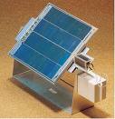
- (Microcontroller Board + Stepper Motor + Sensors)
- Automatic Room Illumination Control (Microcontroller Board + Sensors)
- Automatic Temperature Measurement and Control (Microcontroller Board + Sensors + LCD)
- Closed loop DC Motor Speed Controller (Microcontroller Board + Sensors + LCD + DC Motor)
- PWM DC Motor Speed Controller (Microcontroller Board + Sensors + LCD + DC Motor)
- Frequency Locked Loop DC Motor Speed Control (Microcontroller Board + Sensors + LCD + DC Motor)
- GPS Navigator/Logger (Microcontroller Board + Memory Card +PC Software)
- RF Control Of Induction/DC/Stepper Motor & Other Industrial Loads
- Voltage/Current/Frequency Reading with IR Remote
- Microcontroller based Heartbeat Monitor with LCD Display.
- The design was carried out through the use of two infrared sensors. The sensors check blood density on the patient's fingertips in order to measure heart rate. The raw data from the sensors is processed by microcontroller and the processed data is sent to LCD display.
- Microcontroller based Heartbeat Monitor with Display On Computer.
- same as above but the processed data is sent to PC.
- uC based Wireless(Radio/IR) Heartbeat Monitor
- uC based Heartbeat Monitoring over GSM Mobile.
- The design was carried out through the use of two infrared sensors. The sensors check blood density on the patient's fingertips in order to measure heart rate. The raw data from the sensors is processed by microcontroller and the processed data is sent to user over GSM modem/mobile
- uC based Wireless Temperature Measurement
- Temperature Measurement over GSM Mobile.
- The purpose of this project is to measure the temperature using LM35 sensor. This temperature is processed by microcontroller and sent to the user over GSM mobile.
- uC based Closed Loop Temperature Control
- Temperature Measurement over GSM Mobile.
- The purpose of this project is to measure the temperature using LM35 sensor. This temperature is processed by microcontroller and sent to the user over GSM mobile.
- uC based Closed Loop Temperature Control
- AC/DC/Stepper Motor Closed Loop Speed Control
- Motor Speed Monitoring over GSM Mobile
- uC based Real Time Clock with (2x16) LCD Display
- uC based Real Time Clock and Multiple Device control based on Time and Date.
- uC based MMC/SD Memory Card Interfacing. (Data Logger)
- uC based MMC/SD Memory Card Interfaceing with FAT File System. (Data Logger)
- DC Voltage and Current Meter With LCD Display
- DC Voltage and Current Meter With PC Display.
- uC based Multiple Device Control based on Change in Input Frequency.
- Multi Channel Frequency Measurement with LCD Display
- Multi Channle Voltage Measurement with LCD Display
- Multi Channle Voltage Measurement with PC Display
- Multi Channel Frequency Measurement with PC Display
- Microcontroller based GPS Navigator with Google Earth Interface and MMC/SD 1GB Card Data Logging
- GPS+GSM based Realtime Bus/Train Location Finder and display on Earth's Map
- Microcontroller based Temperature Measurement and Relay Control with PC Interface
- Microcontroller to PC USB Interface With Device Control + PC Software (.NET or VC++)
- uC to PC Serial Interface With Device Control + PC Software (.NET or VC++)
- GPS Compass
- Wireless SCADA
- Wireless Heartbeat Sensor (GSM based)
- Standalone Heartbeat Data Logger (MCU+SD/MMC 1GB Card+Sensors)
The purpose of this project is to log the heartbeat data into the MMC memory stick. The data for the duration upto One Month can be logged continuously
- GSM Based Irrigation System
- Microcontroller Based Temperature Monitoring & Control
- Function Generator Using Microcontroller
- Microcontroller based Substation Monitoring and control System
- Microcontroller based Generator/Alternator Control and Monitoring System.
- Electrical Data (voltage, current, frequency etc...) Logger (SCADA)
- Microcontroller based Single phasing preventor.
- Automatic Rotor Resistance Controller using Microcontroller
- Digital Vehicle Dash Board
- PIR Sensor based Intrusion Detection System
- PIR + GSM based Home Security System
- PC Controlled Digital Devices
- PC Controlled Analog Devices
- Microcontroller to PC Iteraction Using VC++ GUI Application
- Microcontroller to PC Iteraction Using VB GUI Application
- Microcontroller to PC Iteraction Using Java Applet based Application
- Microcontroller to Microcontroller Infrared based communication.
- Solar data logger into MMC/SD Memory Card.
- Microcontroller based refrigeration control system.
- Temperature Analyzers with computerized graphical image.
- Interfacing. Microcontroller to Cellphone graphical display.
- DS1307 and Microcontroller based TV remote controlled Digital Clock.
- Microcontroller based Hardware(USB or Serial) key implementation for any software based applications.
- Microcontroller and GPS based geographical map drawing instrument. Very useful for Civil engineers.
- Microcontroller Digital Access Control System
- Password protected IR based Device Control
- Password protected GSM based Device control
- Remote Control of PC/Computer using GSM Modem or Cell Phone.
- Microcontroller based automatic liquid dispensing system. Used in Tea/Coffee, Soft Drink vending machines.
- Usb 2.0 Hardware implimentation using PIC 18F2550/18F4550 16-bit advanced microcontroller. (With PC side VC++ application).
- GSM+GPS based school kids tracking system.
- Microcontroller based Automatic Railway Gate Control System.
This project is to control the railway gate system automatically by sensing the train movement. This gives the visual and voice alerts to users crossing the rail path. This can also count the number of trains passings in both directions per day or hour.
- Wireless Digital Camera Controller.
Using this project the digital camera can be controlled remotely using RF Transmitter and Receiver. The controls include taking picture snaps, switching on the flash light, changing camera direction using stepper motor etc.
Note: Digital Camera also will be given to the students along with microcontroller hardware kit.
- GSM based Highway vehicle traffic monitoring system.
The purpose of this project is to monitor the vehciles moving on highways at remote locations. This project uses infrared/laser sensor system to count the number of vehicles passing in both the directions. The vehicle count is logged by the microcontroller. This vehicles information is sent to the user over GSM modem. The information can be sent to the user periodically or can be sent on demand by sending a missed call or SMS.
- Zigbee and Touchscreen Controlled PC.
- Advanced vehicle tracking and automatic crash notification using GPS and GSM technology with Location Name as SMS.
- Touchscreen based Ordering System for Restaurants.
- Wearable technology for wireless gadgets control.
- Touchscreen based wireless communication assistant for dumb/illiterates in Airlines.
- Microcontroller and Triac based realtime temperature monitoring and control
- Design and Construction of MEMS Accelerometer based Tilt Operated touch free mobile phone.
- RFID and GSM based intelligent courier/letter collection box.
- MEMS Accelerometer based Tilt Operated wireless phonebook copying to PC.
- Wireless touchscreen based multi-patient health monitoring system for corporate hospitals.
- Wireless PC based multi-patient health monitoring system for Corporate Hospitals.
- GPS & GSM based Human Health Monitoring and Alert System with patient’s location on earth.
- Intelligent mobile phone with GPS enabled features.
- Radio Frequency based wireless remote controlled digital camera with high power focus LED
- Touchscreen based Wireless Language Translator in Airlines using Zigbee.
- Dual GSM Modems based irrigation water pump controller for illiterates.
- Zigbee based Wireless Energy Meter reading system.
- Zigbee based Wireless Energy Meter reading logging system on PC.
- Microcontroller based Wireless matchbox with digital lantern.
DEAD-TIME ELIMINATION FOR VOLTAGE SOURCE INVERTERS
A novel dead-time elimination method is presented in this paper for voltage source inverters. This method is based on decomposing of a generic phase-leg into two basic switching cells, which are configured with a controllable switch in series with an uncontrollable diode. Therefore, dead-time is not needed. In comparison to using expensive current sensors, this method precisely determines the load current direction by detecting which anti-parallel diode conducts in a phase-leg. A low-cost diode-conduction detector is developed to measure the operating state of the anti-parallel diode. In comparison with complicated compensators, this method features simple logic and flexible implementation. This method significantly reduces the output distortion and regains the output RMS value. The principle of the proposed dead-time elimination method is described in detail. Simulation and experimental results are given to demonstrate the validity and features of this new method.
- Introduction
To avoid shoot-though in voltage source inverters (VSI), dead-time, a small interval during which both the upper and lower switches in a phase-leg are off, is introduced into the standard pulse width modulation (PWM) control of VSIs. However, such a blanking time can cause problems such as output waveform distortion and fundamental voltage loss in VSIs, especially when the output voltage is low.
To overcome dead-time effects, most solutions focus on dead-time compensation by introducing complicated PWM compensators and expensive current detection hardware. In practice, the dead-time varies with the gate drive path propagation delay, device characteristics and output current, as well as temperature, which makes the compensation less effective, especially at low output current, low frequency, and zero current crossing. Several switching strategies for PWM power converters have been proposed to minimize the dead-time effect. A dead-time minimization algorithm was also discussed earlier to improve the inverter output performance. A phase-leg configuration topology proposed prevented shoot through. However, an additional diode in series in the phase-leg increases complexity and causes more loss in the inverter. Also, this phase-leg configuration is not suitable for high-power inverters because the upper device gate turn-off voltage is reversely clamped by a diode turn on voltage. Such a low voltage, usually less than 2 V, is not enough to ensure that a device is in its off-state during the activation of its complement device.
High-power inverters usually need longer dead-time than those low-power counterparts. Also due to complicated structures and severe parasitic parameter variations, in practice, the dead-time for high-power inverters requires specific adjustment and/or compensation, and usually this process is time-consuming. For general applications, automatically eliminating dead-time by gate drive technology is a desired and complete solution. Gate drives with intelligent functions are in high demand due to the emerging technology of power electronics building blocks (PEBB) and intelligent power modules (IPM) because smart functions can improve power devices’ modularity, flexibility and reliability.
In this work, an effective dead-time elimination method is proposed. This method is based on decomposing of a generic phase-leg into two basic switching cells, which are configured with a controllable switch in series with an uncontrollable diode. Therefore, dead-time is not needed. In this paper, the effect of dead-time in VSIs will be first introduced. The principle of the proposed method to eliminate dead-time effect is explained in detail. Simulation and experimental results are provided to demonstrate the validity and features of the proposed novel method. Flexible implementation methods are also discussed.
Mechanical Projects
- ROBOTIC ARM INTERFACING WITH PC/MCU/ IR/RF
- HYDRAULIC LIFT
- HYDRAULIC JACK MACHINE
- LINE FOLLOWER OR TRACING ROBOT
- AUTOMATED WALKING ROBOT
- DIGITAL SPEED MEASUREMENT SYSTEM FOR AUTOMOBILE
- LIFT CONTROL USING PC AND MCU
- ESCALATOR LIFT USING PC & MCU
- PATH FINDER MOBILE ROBOT
- MULTILEVEL CAR PARKING LIFT USING MCU
- AUTOMATIC RAILWAY CROSSING GATE CONTROLLER
- AUTO REJECTION + CONVEYER BELT SYSTEM
- AUTO JACK MACHINE
- AUTO BRACK SYSTEM FOR AUTOMOBIL
- PADDLE CONTROLLED WASHING MECHINE
- HYDRO ELECTRICITY
- WIND ELECTRICITY
- ELECTRICITY FROM SPEED BRAKER
- SOLAR SUN SEEKER
- ROBOTIC CRANE WITH UP/DOWN & CIRCULAR MOTION
- AUTO GRASS CUTTER
- HYDRAULIC ROBOTIC ARM
- WALKING ROBOT
PC Based Projects
- PC TO PC COMMUNICATION USING IR/FIBER OPTIC CABLE
- PWM CONTROL OF DC MOTOR USING C++
- COMPUTERISED ELECTRICAL APLAINCE CONTROL
- DATA ACQUISITION CARD FOR P.C.
- SIMPLE ANALOGUE INTERFACE FOR P.C.
- P.C. BASED FUNCTION GENERATOR
- PC BASED SUN SEEKER
- COMMUNICATION BETWEEN PC’S USING IR, LASER
- SIMPLE RELAY AND SENSOR INTERFACE FOR P.C.
- P.C. BASED DIGITAL CLOCK
- INTERFACE YOUR PC WITH LIGHT AND FANS
- P.C. BASED VISITOR COUNTER
- P.C. BASED TOKEN NUMBER DISPLAYER
- PC BASE TRANSISTOR LEAD IDENTIFIER
- PC BASED STEPPER MOTOR CONTROLLER
- PC BASED DC MOTOR SPEED CONTROLLER
- P.C. BASED 7-SEGMENT ROLLING DISPLAY
- PC. BASED DC MOTOR SPEED CONTROLLED
- PC BASED ROBOTIC ARM
- P.C. BASED TIMER
- P.C. BASED MULTILEVEL CAR PARKING
TOUCH SCREEN seminar
First computers became more visual, then they took a step further to understand vocal commands and now they have gone a step further and became ‘TOUCHY’, that is skin to screen.
A touchscreen is an easy to use input device that allows users to control PC software and DVD video by touching the display screen. A touch system consists of a touch Sensor that receives the touch input, a Controller, and a Driver. The most commonly used touch technologies are the Capacitive & Resistive systems. The other technologies used in this field are Infrared technology, Near Field Imaging & SAW (surface acoustic wave technology). These technologies are latest in this field but are very much expensive.
The uses of touch systems as Graphical User Interface (GUI) devices for computers continues to grow popularity. Touch systems are used for many applications such as ATM’s, point-of–sale systems, industrial controls, casinos & public kiosks etc. Touch system is basically an alternative for a mouse or keyboard.
The market for touch system is going to be around $2.5 billion by 2004. Various companies involved in development of touch systems mainly are Philips, Samsung etc. Even touch screen mobile phones have been developed by Philips.
INTRODUCTION
A touchscreen is an easy to use input device that allows users to control PC software and DVD video by touching the display screen. We manufacture and distribute a variety of touch screen related products.
A touch system consists of a touch
Sensor that receives the touch input, a Controller, and a Driver. The touch screen sensor is a clear panel that is designed to fit over a PC. When a screen is touched, the sensor detects the voltage change and passes the signal to the touch screen controller. The controller that reads & translates the sensor input into a conventional bus protocol (Serial, USB) and a software driver which converts the bus information to cursor action as well as providing systems utilities.
As the touch sensor resides between the user and the display while receiving frequent physical input from the user vacuum deposited transparent conductors serve as primary sensing element. Vacuum coated layers can account for a significant fraction of touch system cost. Cost & application parameters are chief criteria for determining the appropriate type determining the system selection. Primarily, the touch system integrator must determine with what implement the user will touch the sensor with & what price the application will support.
Applications requiring activation by a
gloved finger or arbitrary stylus such as a plastic pen will specify either a low cost resistive based sensor or a higher cost infra-red (IR) or surface acoustic wave (SAW) system. Applications anticipating bare finger input or amenable to a tethered pen comprises of the durable & fast capacitive touch systems. A higher price tag generally leads to increased durability better optical performance & larger price.
The most commonly used systems are
generally the capacitive & resistive systems. The other technologies used in this field are Infrared technology & SAW (surface acoustic wave technology) these technologies are latest in this field but are very much expensive.
MICROCONTROLLER BASED PROJECTS
- WIRELESS MESSAGING VIA MOBILE/LANDLINE
- GSM BASE HOME SECUIRTY SYSTEM
- GSM BASED HOMEAUTOMATION & SECUIRTY
- AUTOMATIC TOLL TAX
- VOTING MACHINE
- SMS BASE DEVICE SWITCH
- SOLAR TARKER SYSTEM
- TEXT DATA COMMUNICATION THROUGH FIBER/LAGER
- DIGITAL COMBINETION LOCK
- SAFETY GUARD FOR THE BLIND (PROXIMITY BASE
- SMS THROUGH TELEPHONE
- SPEED CHECKER FOR HIGHWAYS
- SMART CARD
- DATA SECUIRTY SYSTEM
- TOUCH SCREEN
- HEART BEAT MONITOR
- AUTOMATIC ROOM LIGHT CONTROLLER:
- RADAR SYSTEM ILIGAL AROPLAN DETECTOR
- PRI-PAID CAR PARKING
- MULI LAVEL CAR PARKING
- FASTEST-FINGER-FIRST USING 89C51
- MICRO PROCESSOR BASED REVERSIBLE D.C. MOTOR CONTROL
- STEPPER MOTOR CONTROL USING 89C51
- MIC-89C51 MONITORING SYSTEM
- MANUAL AT 89C51 PROGRAM
- AT 89C2051 BASED COUNTDOWN TIMER
- MICROCONTROLLER BASED CODE LOCK USING AT 89C2051
- LCD FREQUENCY METER USING 89C2051
- CALLER ID UNIT USING MICRO-CONTROLLER
- MICROPROCESSOR-BASED HOME SECURITY SYSTEM
- STEPPER MOTOR CONTROL USING 89C51 MICRO-CONTROLLER
- MICRO CONTROLLER BASED TEMPERATURE METER
- MICRO CONTROLLER BASED HEARTBEAT MONITOR
- ULTRASONICRANGEFINDER USING PIC MICRO CONTROLLER
- CALLER- ID UNIT USING MICRO CONTROLLER
- MICRO CONTROLLER BASED PATHFINDER
- MICRO CONTROLLER BASED ROBOT.
- MICRO CONTROLLER MOVING MESSAGE DISPLAY
- MICRO CONTROLLER BASED RELAY SWITCHING
- MICRO CONTROLLER AUTO DIALER USING GSM.
- MICRO CONTROLLER BASED WATER LEVER INDICATOR
- MICRO CONTROLLER BASED WIRELESS HOME AUTOMATION
- MICROCONTROLLER BASED RADAR SYSTEM
- MULTI CHANNEL INFRA RED CONTROL 4 different point 89c2051 micro controller in transmitter and receiver, using infra red technique.
- MOVING MESSAGE DISPLAY : 89c51 micro controller Led matrix,
- Digital clock with alarm: using 89c51 micro controller
- TRAFFIC LIGHT WITH DOWN COUNTER : all the four sides of the road with one side counter display using 89c51 micro controller circuit.
- ULTRASONIC DISTANCE METER USING MICROCONTROLLER
- PRI-PAID CAR PARKING SYSTEM
- MICRO CONTROLLER TEMPERATUIRE METER
- ANOLOG TO DIGITAL CONERTER USING AT89C51 MCU
- INFARED REMOTE CONTROLE SYSTEM
- ULTRASONIC MOVEMENT DETECTOR
- MICROCONTROLLER BASED TACHOMETER
- MCU BASED VISITOR COUNTER
- PWM CONTROL OF DC MOTOR USING 89C51
- AN INTELLIGENT AMBULANCE CAR WHICH CONTROL TO TRAFFIC LIGHT
- PRE-PAID ENERGY METER
- MICROC CONTROLLER BASED LINE FOLLOWER OR TRACING ROBOT
- AUTOMATED WALKING ROBOT CONTROLLED BY MCU
- AUTO BRAKING SYSTEM
- AUTOMATIC RAILWAY CROSSING GATE CONTROLLER
- BLUETHOOTH BASED HOME AUTOMATIONl
- BLUETHOOTH BASED DATA COMMUNICATION
- CLASS ROOM ADDRESSING SYSTEM
- RESTARURANT ORDERIN SYSTEM
- MINES DETECTOR ROBOT
- AUTOMATIC RAIRWAY CROSSING GATE CONTROLLER AND TRACK SWITCHING
list of projects for final year students electronics\communication\instrumemtation\ and control
- DIGITAL COMBINETION LOCK
- SAFETY GUARD FOR THE BLIND (PROXIMITY BASE)
- LIGHT COTROLLED DIGITAL FAN REGULATOR
- LOW-COST ENERGY METER USING ADE 7757
- HOME AUTOMATION AND SECURITY CONTROL INTERFACE WITH TELEPHONE
- LINE TRACKING ROBOT/MOUSE
- REMOT CONTROLLED STEPPER MOTOR
- ULTRASONIC SWITCH
- DEVICE SWITCHING USING PASSWORD
- SPEED CHECKER FOR HIGHWAYS
- ULTRASONIC PROXIMITY DETECTOR
- ULTRASONIC MOVEMENT DETECTOR
- VEHICLE SEED MEASUREMENT CONTROL PC BASED
- SMART CARD FOR ENTRY EMPLOY
- SECURITY ACCESS CONTROL SYSTEM
- RADAR SYSTEM
- PRI-PAID ENERGY METER
- PRI-PAID CAR PARKING SYSTEM
- ULTRASONIC DISTANCE METER
- DATA SECUIRTY SYSTEM
- DESIGN OF A BUS STATUS IDENTIFICATION SYSTEM
- CALLING NUMBER IDENTIFICATION USING CALCULATOR
- OPTICAL REMOT SWITCH
- LOAD PROTECTOR WITH REMOTE SWITCHING
- DISITAL WEIGHT ACCUMULATOR
- REMOT CONTROLLED LAND ROVER
- TELEPHONE ANSIRING MATCHING
- AUTO CAR PARKING
- AN INTELLIGENT AMBULANCE CAR WHICH CONTROL TO TRAFFIC LIGHT
- WATCHMAN ROBOT
- SUN SEEKER
- AUTO BRAKING SYSTEM
- TOUCH SCREEN
- DTMF REMOTE CONTROL SYSTEM
- AUTOMATIC RAILWAY CROSSING GATE CONTROLLER
- HOME SECURITY SYSTEM WITH SENDING MESSAGE ON OUR CELL PHONE
- FASTED FINGER FIRST
- MOBILE CONTROL ELECTRICAL APPLIANCES
- RF CONTROL ELECTRICAL APPLIANCES
- MIND READER
- DIGITAL COMBINATION LOCK
- SAFETY GUARD FOR THE BLIND
- DIGITAL SPEEDOMETER
- RADIO CONTROLLED REMOTE CONTROL
- MICRO PROCESSOR-BASED DC MOTOR SPEED CONTROL
- 31/2 DIGIT VOLTMETER WITH LED
- 31/2 DIGIT VOLTMETER WITH LCD
- 31/2 DIGIT THERMOMETER
- DTMF 5-CHANNEL SWITCHING VIA POWER LINE
- DEVICE SWITCHING USING PASSWORD
- LASER-BASED COMMUNICATION LINK
- VIOCE & DATA COMMUNICATION WITH FIBER LINK
- BUDGET DIGITAL OSCILLOSCOPE
- WIRELESS HOME SECURITY
- BEND STOP FILTER
- A VERSATILE FUNCTION GENERATOR
- DIGITAL DOOR BELL
- TRANSFORMER LESS 12V DUAL POWER SUPPLY
- INFRARED BURGLAR ALARM WITH TIMER
- AUTOMATIC VOLTAGE STABILIZER USING AUTOTRANSFORMER
- DIGITAL CODE LOCK
- TELEPHONE CALL METER
- EMERGENCY LIGHT USING CFL
- WIDE RANG SQUARE WAVE GENERATOR
- 1 HZ CLOCK GENERATOR
- REMOTE MUSICAL BELL
- ELE. TELEPHONE DEMONSTRATOR
- TELEPHONE CALL COUNTER
- LED VOLTMETER FOR CAR BATTERY
- QUALITY FM TRANSMITTER
- DIGITAL VOLUME CONTROL
- 99.99 SEC. STOP-CLOCK
- MULTIPURPOSE DIGITAL COUNTER
- VERSATILE ON/OFF TIMER
- SUPER SIMPLE TRIANGULAR TO SINE WAVE GENERATOR
- DIGITAL FAN REGULATOR
- TEMPERATURE DISPLAY
- FREQUENCY GENERATOR
- SOUND LEVEL INDICATOR FOR STEREO SYSTEM
- SINGLE-GATE SQUARE WAVE GENERATOR
- QUICK 741 AND 555 TESTER
- REGULATE DUAL POWER SUPPLY
- SENSITIVE FM TRANSMITTER
- LIGHT CONTROLLED DIGITAL FAN REGULATOR
- MOVING MESSAGE DISPLAY EPROM BASE
- PROGRAMMABLE DIGITAL TIME SWITCH
- PROGRAMMABLE DIGITAL TIMER CUM CLOCK
- REMOTE CONTROL AUDIO PROCESSOR
- HEART BEAT MONITOR
- AROPLANE DIRECTION INDICATOR
- VOICE TRANSMITTER IN POWER LINE AND SWITCHING
- A SINGLE-CHIP TIMER WITH DIGITAL CLOCK AND CALENDER
- IMPEDANCE METER
- REMOTE AUDIO LEVEL INDICATOR
- MULTICHANNEL TOUCH SWITCH
- SAW TOOTH WAVE GENERATOR
- TEMPERATURE CONTROLLED FAN
- 1 HZ MASTER OSCILLATOR
- REMOTE TV TESTER
- CORDLESS INTERCOM
- REMOT CONTROLLERED LAND FOVER –A DIY ROBOTIC PROJECT
- DIGITAL WEIGHT ACCUMULATOR
- IR- TO- RF CONVERTER
- FM RECEIVER USING CXA1619
- HEAT SENSITIVE SWITCH
- TRANSISTOR TESTER
- AUTOMETIC SCHOOL BELL
- DIGITAL STOP WATER
- INFRARED INTERUPTION COUNTER
- AUTOMATIC ROOM LIGHT CONTROLLER: In this project we use object counter circuit with, auto light on when any body enter in the room and counter display any number, when all the person left the room and counter shows a 0 number on display then only light is off two rays of sensor is install in the door.
AUTOMATIC RAILWAY TRACK SWITCHING USING STEPPER MOTOR CONTROL
SMART ENERGY METER WITH MICRO CONTROLLER
ADAPTIVE TRAFFIC CONTROL
ULTRASONIC RANGE DETECTOR project
Saturday, 4 September 2010
PWM Dimmer/Motor Speed Controller
 Photo of Completed PWM Dimmer/Speed Control
The photo shows what a completed board looks like. Dimensions are 53 x 37mm, so it’s possible to install it into quite small spaces. The parts used are readily available, and many subsitiutions are available for both the MOSFET and power diode (the latter is only needed for motor speed control). The opamps should not be substituted, because the ones used were chosen for low power and their ability to swing the output to the negative supply rail.
Note that if used as a motor speed controller, there is no feedback, so motor speed will change with load. For many applications where DC motors are used, constant speed regardless of load is not needed or desirable, but it is up to you to decide if this will suit your needs.
Description
First, a description of PWM is warranted. As the pot is rotated clockwise, the input voltage changes linearly with rotation. At first, the voltage is such that the comparator output is just narrow spikes, which turn the MOSFET on for a very short period. Average current is low, so connected LEDs will be quite dim, or a motor will run (relatively) slowly. As the input voltage coming from the pot increases, the MOSFET is on for longer and longer, so increasing power to the load.
 Figure 1 – PWM Waveform Generation
Figure 1 shows how the PWM principle works. The red trace is the triangle wave reference voltage, and the green trace is the voltage from the pot. When the input voltage is greater than the reference voltage, the MOSFET turns on, and current flows in the load. Because the frequency is relatively high (about 600Hz), we don’t see any flicker from the LEDs, but the tone is audible from a motor that’s PWM controlled. The PWM signal is shown in blue. The average current through the load is determined by the ratio of on-time to off-time, and when both are equal, the average current is exactly half of that which would be drawn with DC.
 Figure 2 – Dimmer/Speed Controller Schematic
The circuit is shown in Figure 2. U1 is the oscillator, and generates a triangular waveform. R4 and R5 simply set a half voltage reference, so the opamps can function around a 6V centre voltage. U2A is an amplifier, and its output is a 10V peak to peak triangle wave that is used by the comparator based on U2B. This circuit compares the voltage from the pot with the triangle wave. If the input voltage is at zero, the comparator’s output remains low, and the MOSFET is off. This is the zero setting.
In reality, the reference triangle waveform is from a minimum of about 1.5V to a maximum of 9.5V, so there is a small section at each end of the pot’s rotation where nothing happens. This is normal and practical, since we want a well defined off and maximum setting. Because of this range, for lighting applications, an industry standard 0-10V DC control signal can be used to set the light level. C-BUS (as well as many other home automation systems) can provide 0-10V modules that can control the dimmer.
While a 1N4004 diode is shown for D2, this is only suitable if the unit is used as a dimmer. For motor speed control, a high-current fast recovery diode is needed, such as a HFA15TB60PBF ultra-fast HEXFRED diode. There are many possibilities for the diode, so you can use whatever is readily available that has suitable ratings. The diode should be rated for at least half the full load current of the motor, and the HFA15TB60PBF suggested is good for 15A continuous, so is fine with motors drawing up to 30A.
Construction
While it’s certainly possible to build the dimmer on veroboard or similar, it’s rather fiddly to make and mistakes are easily made. Also, be aware that because of the current the circuit can handle, you will need to use thick wires to reinforce some of the thin tracks. This is even necessary for the PCB version. Naturally, I recommend the PCB, and this is available from ESP. The board is small – 53 x 37mm, and it carries everything, including the screw terminals. The PCB is double-sided with plated-through holes, and has solder masks on both sides.
The MOSFET will need a heatsink unless you are using the dimmer for light loads only. It is necessary to insulate the MOSFET from the heatsink in most cases, since the case of the transistor is the drain (PWM output). For use at high current and possible high temperatures, the heatsink may need to be larger than expected. Although the MOSFET should normally only dissipate about 2W or so at 10A, it will dissipate a lot more if it’s allowed to get hot. Switching MOSFETs will cheerfully go into thermal runaway and self destruct if they have inadequate heatsinking. You may also use an IGBT (insulated gate bipolar transistor) – most should have the same pinouts, and they do not suffer from the same thermal runaway problem as MOSFETs.
As noted above, there are many different MOSFETs (or IGBTs) and fast diodes that are usable. The IRF540 MOSFET is a good choice, and being rated 27A it has a generous safety margin. There are many others that are equally suitable – in fact any switching MOSFET rated at 10A or more, and with a maximum voltage of more than 20V is quite ok.
Dual Power Amplifier Using TDA7293 MOSFET IC
As readers will know, there are already several power amplifier projects, two using IC power amps (aka power opamps). Both have been popular, and this project is not designed to replace either of them. However, it is significantly smaller than the others, so it makes building a multiple amp unit somewhat easier because the space demand is much lower. It's quite simple to include 4 amps (two boards) into a small space, but be aware that good heatsinking is essential if you expect to run these amps at significant power levels.

Photo of Completed P127 Board
The TDA7293 IC uses a MOSFET power stage, where the others featured use bipolar transistors. The main benefit of the MOSFET stage is that it doesn't need such radical protection circuitry as a bipolar stage, so unpleasant protection circuit artefacts are eliminated. There are no apparent downsides to the TDA7293, although it was found that one batch required a much higher voltage on the Standby and Mute pins than specified, or the amps would not work. This is not a limitation, since both are tied to the positive supply rail and are therefore disabled.
This particular project has been planned for a long time, but for some reason I never got around to completing the board or the project description. This is now rectified, and it's ready to "rock and roll". The board is very small - only 77 x 31mm, so getting it into tight spaces is easy ... provided adequate heatsinking is available of course.
Description
The TDA7293 has a bewildering number of options, even allowing you to add a second power stage (in another IC) in parallel with the main one. This improves power into low impedance loads, but is a rather expensive way to get a relatively small power increase. It also features muting and standby functions, although I've elected not to use these.
The schematic is shown in Figure 1, and is based on the PCB version. All unnecessary functions have been disabled, so it functions as a perfectly normal power amplifier. While the board is designed to take two TDA7293 ICs, it can naturally be operated with only one, and the PCB is small enough so that this is not an inconvenience. A LED is included to indicate that power is available, and because of the low current this will typically be a high brightness type.

Figure 1 - Schematic of Power Amplifier (One Channel Shown)
The IC has been shown in the same format that's shown in the data sheet, but has been cleaned up for publication here. Since there are two amps on the board, there are two of most of the things shown, other than the power supply bypass caps and LED "Power Good" indicator. These ICs are extremely reliable (as are most power amp ICs), and to reduce the PCB size as much as possible, fuse clips and fuses have not been included. Instead, there are fusible tracks on the board that will fail if there is a catastrophic fault. While this is not an extremely reliable fuse, the purpose is to prevent power transformer failure, not to protect the amplifiers or PCB.
I normally use a gain of 23 (27dB) for all amplifiers, and the TDA7293 is specified for a minimum gain of 26dB, below which it may oscillate. Although this is only a small margin, tests so far indicate that the amp is completely stable. If you wish, you may increase the gain to 28 (29dB) to give a bit more safety margin. To do this, just change the input and feedback resistors (R3A/B and R4A/B) from 22k to 27k.
The circuit is conventional, and is very simple because all additional internal functions are unused. The LED is optional, and if you don't think you'll need it, it may be omitted, along with series resistor R3. All connections can be made with plugs and sockets, or hard wired. In most cases, I expect that hard wiring will be the most common, as the connectors are a pain to wire, and add unnecessary cost as well as reduce reliability.
The TDA7293 specifications might lead you to believe that it can use supply voltages of up to ±50V. With zero input signal (and therefore no output) it might, but I don't recommend anything greater than ±35V if 4 ohm loads are expected, although ±42V will be fine if you can provide good heatsinking. In general, the lower supply voltage is more than acceptable for 99% of all applications, and higher voltages should not be used unless there is no choice. Naturally, if you can afford to lose a few ICs to experiments, then go for the 42V supplies (obtained from a 30+30V transformer).
This amp can also be bridged, using the Project 87 balanced transmitter board. You can expect about 150W into 8 ohms from a +/-35V supply. It cannot be bridged into 4 ohms, as the effective impedance on each amplifier is too low.
Construction
Because of the pin spacings, these ICs are extremely awkward to use without a PCB. Consequently, I recommend that you use the ESP board because it makes building the amplifier very simple. The PCBs are double sided with plated-through holes, so are very unforgiving of mistakes unless you have a good solder sucker. The best way to remove parts from a double sided board is to cut the pins off the component, then remove each pin fragment individually. This is obviously not something you'd wish to do if a power amp IC were installed incorrectly, since it will be unusable afterwards.

Figure 2 - TDA7293V Pinouts
The diagram above shows the pinouts for the TDA7293V (the "V" means vertical mounting). Soldering the ICs must be left until last. Mount the ICs on your heatsink temporarily, and slide the PCB over the pins. Make sure that all pins go through their holes, and that there is no strain on the ICs that may try to left the edge off the heatsink. When ICs and PCB are straight and aligned, carefully solder at least 4 pins on each IC to hold them in place. The remaining pins can then be soldered. Remember, if you mess up the alignment at this point in construction, it can be extremely difficult to fix, so take your time to ensure there are no mistakes.
This amplifier must not be connected to a preamp that does not have an output coupling capacitor. Even though there is a cap in the feedback circuit, it can still pass DC because there is no input cap on the PCB. I normally include an input cap, but the goal of this board was to allow it to fit into the smallest space possible, and the available board space is not enough to include another capacitor. A volume control (typically 10k log/ audio taper) may be connected in the input circuit if desired.
Note that the metal tab of the TDA7293 is connected to the -Ve supply, so must be insulated from the heatsink. The more care you take with the mounting arrangement, the better. While you can use a screw through an insulating bush and a piece of mica to insulate the tab, a better alternative is to use a clamping bar of some kind. How you go about this depends a lot on your home workshop tools and abilities, but one arrangement I've found highly satisfactory is a suitable length of 6.25mm square solid steel bar. This is very strong, and allows good pressure on the mica (or Kapton) for maximum heat transfer. Naturally, heatsink compound is absolutely essential.
Do not be tempted to use silicone insulation washers unless you are using the amp at very low supply voltages (no more than ±25V). Its thermal transfer characteristics are not good enough to allow the amp to produce more than about 10 - 20W of music, and even that can be taxing for silicone washers. The amp will shut down if it overheats, but that curtails one's listening enjoyment until it cools down again.
Friday, 3 September 2010
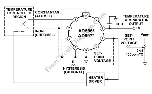
Setpoint Voltage of AD597 is °C × 10.1mV/°C – 9.1mV and Setpoint Voltage of AD596 is °C × 9.6mV/°C + 42mV. The setpoint pin of the AD596/AD597 has input impedance of about 50k. This resistance has temperature coefficient of ±15ppm/°C. This device has an additional ±1°C degradation of temperature stability over the +25°C to +100°C ambient temperature range due to 100ppm/°C 5k pot.
To increase system reliability and provide noise immunity, this device use Switching hysteresis. to enhanced system reliability, mechanical component wear is reduced by reducing the frequency of on-off cycling. It can be done by adding a single external resistor between Pins 7 and 3 of the AD596/AD597. The hysteresis is determined by following equation:
Rhyst=(Vout/200nA)*(1/°Chyst)
The alarm transistor will be ON regardless of whether there is an open circuit or not because the AD596/AD597 output is saturated at all times. for proper operationof the rest of the circuit, -ALM must be tied to a voltage below (+Vs – 4V) [Circuit's schematic diagram source: analog.com]
ieee projects free download
| Project | Author |
|---|---|
Smart Vehicles In this project, students learn how making automobiles more autonomous can make them safer, by providing functionality like anti-lock braking, self parallel parking, and lane departure warnings. In the laboratory, the students work with small motorized cars with infrared sensors, programming the cars to spin in a circle, stop on a line, and follow a curvy path. In the process, the students learn about infrared sensors, motors, and embedded systems. A code framework is provided so that minimal programming skills are required. In this project, students learn how making automobiles more autonomous can make them safer, by providing functionality like anti-lock braking, self parallel parking, and lane departure warnings. In the laboratory, the students work with small motorized cars with infrared sensors, programming the cars to spin in a circle, stop on a line, and follow a curvy path. In the process, the students learn about infrared sensors, motors, and embedded systems. A code framework is provided so that minimal programming skills are required.» View All Project Files | Leyla Nazhandali |
Manipulating Everyday Objects with Prosthetic Hands In this project, students learn how prostheses that use robotic technology can improve the lives of people with disabilities. In the laboratory, the students use Lego Mindstorms NXT kits to create an artificial arm or hand that can lift small objects, such as a coffee cup. In the process, students discover and explore the following concepts and ideas: Hooke's Law, hysteresis, Newton's Second Law, accuracy and precision, rapid prototyping, and the relationship between the voltage applied to a motor and its speed. In this project, students learn how prostheses that use robotic technology can improve the lives of people with disabilities. In the laboratory, the students use Lego Mindstorms NXT kits to create an artificial arm or hand that can lift small objects, such as a coffee cup. In the process, students discover and explore the following concepts and ideas: Hooke's Law, hysteresis, Newton's Second Law, accuracy and precision, rapid prototyping, and the relationship between the voltage applied to a motor and its speed.» View All Project Files | Chris Macnab |
Error Correction Codes for Wireless Communication Systems In this project, students learn how error correction coding makes wireless communications more robust in the presence of noise. In the laboratory, the students work in Matlab to code two simple error correction schemes, and simulate their use in a wireless channel. In the process, they learn concepts such as bit error rate, and see the trade-off between processing time and robustness. In this project, students learn how error correction coding makes wireless communications more robust in the presence of noise. In the laboratory, the students work in Matlab to code two simple error correction schemes, and simulate their use in a wireless channel. In the process, they learn concepts such as bit error rate, and see the trade-off between processing time and robustness.» View All Project Files | Sami Khorbotly |
Solid State Lighting for the Developing World In this project, students learn how solid state lighting technology can improve the lives of people in the developing world, making their evenings more productive and safer. In the laboratory, the students design a portable, solar-charged, LED lamp that can provide two hours of reading light. In the process, they learn about basic circuits, the engineering design cycle, and light. They also compare the efficiency, durability, and cost of lighting technologies. In this project, students learn how solid state lighting technology can improve the lives of people in the developing world, making their evenings more productive and safer. In the laboratory, the students design a portable, solar-charged, LED lamp that can provide two hours of reading light. In the process, they learn about basic circuits, the engineering design cycle, and light. They also compare the efficiency, durability, and cost of lighting technologies.» View All Project Files | Loren Wyard-Scott |
Energy System Design: A Look at Renewable Energy In this project, students learn how harvesting energy from renewable sources will help meet the future needs of society. In the laboratory, the students will develop a system to store energy from a renewable source (represented in the laboratory by a light bulb, a box fan, or flowing water). The students will transport the energy, and use it to supply an electrical load (a light bulb) in a different physical location. In the process, students will learn about energy and power, and will learn about In this project, students learn how harvesting energy from renewable sources will help meet the future needs of society. In the laboratory, the students will develop a system to store energy from a renewable source (represented in the laboratory by a light bulb, a box fan, or flowing water). The students will transport the energy, and use it to supply an electrical load (a light bulb) in a different physical location. In the process, students will learn about energy and power, and will learn aboutanalysis of physical systems, modeling and simulation, and design under constraints. » View All Project Files | Taryn Bayles |
Feedback Controlled Brushless DC Motor with Personal Electric Vehicle Application In this project, the students learn how brushless DC motors have made personal electric vehicles (PEVs) possible, and calculate how much using a PEV instead of an automobile for some of their daily driving can impact their production of carbon dioxide, based on United States driving patterns. In the laboratory, students build a brushless DC motor using three different control methods, based on a reed switch, a Hall effect sensor, and optoelectronics, respectively. In the process, students learn about motors, and compare the components used for control in terms of their reliability. In this project, the students learn how brushless DC motors have made personal electric vehicles (PEVs) possible, and calculate how much using a PEV instead of an automobile for some of their daily driving can impact their production of carbon dioxide, based on United States driving patterns. In the laboratory, students build a brushless DC motor using three different control methods, based on a reed switch, a Hall effect sensor, and optoelectronics, respectively. In the process, students learn about motors, and compare the components used for control in terms of their reliability.» View All Project Files | Stephen Williams |
| Human Energy Generation and Electrical Signal Measurement In this project, students learn about the energy generation and usage. Emphasis is placed on potential sources of renewable energy, and on how power demands vary from country to country. The students learn how energy is measured, and experiment with generating and storing energy themselves, using an AC generator connected to a bicycle and lead-acid batteries. They measure how long common household appliances can be run on the stored energy, and in the process gain a better understanding of their own personal energy usage. » View All Project Files | Tom Hartley |
| Pico Power Generation for the Developing World In this project, students create a power source capable of providing 1 Watt-hour of energy for night-time use. The students learn how access to even a small source of electrical power can make a difference to families in remote, undeveloped areas of the world. They also learn some basics of circuits, energy, and motors and generators, and gain experience with an engineering development process. » View All Project Files | Loren Wyard-Scott |
| Map Mashups for Better Visualization of Location-Based Trends In this project, students learn that map mashups can help improve understanding of a societal problem by allowing better visualization of location-based trends; for example, map mashups can be used to show the spread of epidemics, or the relative rates of child poverty, color coded on a map in an interactive and graphical way. The students learn how to program a map mashup, using the Google Maps API. In the process, they learn about object-oriented programming and web applications. Two versions of the project are provided, for students with and without prior experience in object-oriented programming (OOP). Version 2, for students with experience in OOP, has been zipped into one file listed under "Additional Project Materials". » View All Project Files | Kamyar Dezhgosha |
| Developing a Personally Controlled Health Record (PCHR) Using Microsoft Visual C# In this project, students learn how personally controlled health records can make it possible for a person to capture, access, and manage his or her own health information in a convenient and secure way. They learn how these records can improve quality of care by improving communication between multiple healthcare providers, and reduce costs by avoiding unnecessary duplication of medical tests. In the laboratory, students use C# to program personally controlled health records. Along the way, they learn programming skills, about how encryption can be used to secure data, and about the design of user-friendly user interfaces. » View All Project Files | Nicky Mostert-Phipps |
| Digital Logic for Medicine and Biology Research: A hardware implementation of the Smith-Waterman algorithm for DNA comparison In this project, students learn that the comparison of DNA sequences is important to a wide variety of applications in medicine and biology, including the analyses of ecosystem biodiversity, cancer mutations and the evolution of viruses. The students learn that specialized yet inexpensive digital hardware based on field programmable gate arrays can help speed the analysis of DNA sequences. They design and test a simple implementation of the Smith-Waterman algorithm that is broadly used for DNA sequence comparisons. In the process, they learn about computational platforms, digital logic, and a divide-and-conquer approach to design. » View All Project Files | Javier Resano |
| Energy Scavenging from Vibrations In this project, students learn that energy can be harvested or scavenged from the surrounding environment, in sufficient quantities for use in powering embedded systems. In the laboratory, students design and build a system using Lego pieces and a piezoelectric buzzer that harvests energy from vibrations and uses the energy to charge a battery. Along the way, the students learn about dc motors, cams and gears, piezoelectric material, and circuits for charging. » View All Project Files | Yanfei Liu |
| Language Identification Software In this project, students learn how it is possible to identify the language in which a text file is written, a necessary first step in automatic translation of information from one language to another. In the laboratory, the students write Java programs to compute histograms of letter frequencies in text files, and explore how letter frequencies vary in Italian, German, and English. Along the way, they learn about ASCII codes, and about how sampling a longer portion of a text takes longer, but produces a more accurate accounting of letter frequency for that text. » View All Project Files | Andrea Mitofsky |
| Embedding Data in Digital Images In this project, students learn how digital watermarking is used to authenticate and protect copyrights in digital multimedia by permanently embedding data (a watermark) in the object of interest that only the original owner can change or remove. In the process, they learn how digital images are represented in binary format and stored, and work in Matlab, becoming familiar with matrices, arrays, and strings, and learning various techniques for data manipulation. » View All Project Files | Sami Khorbotly |
| Electrocardiogram Amplifier Design Using Basic Electronic Parts This project is broadly centered around the topic of biomedical circuits. Its overall aim is to provide biomedical or electronic engineering students with a hands-on opportunity to develop an electrocardiogram (ECG) amplifier circuit from scratch and thereby learn more about the technical details of bio-potential measurement devices. » View All Project Files | Alfred Yu |
| The Coding of Sound by a Cochlear Prosthesis In this project, students learn how cochlear implants work to improve the lives of people with profound hearing loss. The students experiment with the control parameters of a cochlear implant signal processor using Matlab tools, and learning digital signal processing concepts, including filtering, along the way. » View All Project Files | Pamela Bhatti |
| Arrhythmia Detection Algorithms for Implantable Cardioverter Defibrillators In this project, students learn how implantable cardioverter defibrillators allow people with certain kinds of cardiac arrhythmias to live normal, active lives. In the laboratory, the students use Matlab to investigate algorithms for quickly and accurately detecting the abnormal heart rhythms that require intervention. Along the way, they learn that signals can be processed in both the time and frequency domains, and how the complexity of an algorithm affects how quickly it runs. They also consider the ethics of an actual case in which a maker of defibrillators discovered a flaw in their device, but delayed publicizing the flaw for three years. » View All Project Files | Amy Bell |

