
I have designed a development board for practicing 8051 microcontrollers. The development board is simple one containing minimum hardware required for a 8051 chip to function. The 8051 chip used in this development board is 89S52. The AT89S52 comes in a 40 pin PDIP package. It consists 8kB in system programmable flash memory for code storage, 256 bytes of RAM, 32 I/O lines, three 16 bit timer/counters, one full duplex serial port and many more. For further details you can refer the datasheet.
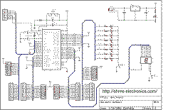
Figure below shows the circuit diagram of the development board. Click on the image to enlarge. I have connected pull up resistors for all the ports in the circuit diagram, but pull ups are compulsory only for port 0. You can neglect pull ups connected for other ports since they are connected to pull ups internally.
This circuit can be easily constructed in a general purpose circuit board. One can neglect the seven segment display and 8 LEDs if they wish to build it separately. I will be publishing the PCB files for this board soon. Keep visiting.
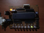
Some Images of my 8051 development board built on breadboard. This is my first version of my board so the 7 segment display is not present.
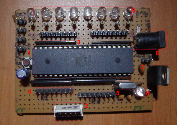
Image notes: 1] The marvel chip Atmel’s 89S52 2] ISP port for downloading programs 3] Pull up resistor network 4] connectors to connect I/O pins to any other circuits/interface boards 5] 11.0592 Mhz crystal 6] Power connector 7] 7805 voltage regulator 8] Power indication LED 9] 8 LEDs connected to Port 0


malisimo flaco
ReplyDelete